Continue to Site

Welcome to EDAboard.com

Welcome to our site! EDAboard.com is an international Electronics Discussion Forum focused on EDA software, circuits, schematics, books, theory, papers, asic, pld, 8051, DSP, Network, RF, Analog Design, PCB, Service Manuals... and a whole lot more! To participate you need to register. Registration is free. Click here to register now.

Bare PCB Tests: Do I save money on the fixture if...

Status
Not open for further replies.

edaenrico

Member level 4
Member level 4
Joined
Apr 19, 2010
Messages
76
Helped
10
Reputation
20
Reaction score
10
Trophy points
1,288
Activity points
1,864
Hi,

I've been wondering if the routing my boards in a certain way makes me save money on the PCB Bare board tests.

I route the board in order to have the minimal number of end points as possible.

Each end point will require a nail in the fixture.
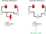
ROUTING-TOPOLOGY.jpg


The questions are:

1) Having fewer nails is good or not for the tests?

2) Do bare PCB tests cost less if the PCB require less nails?


Thanks,
Enrico Migliore
 

The questions are:

1) Having fewer nails is good or not for the tests? (less test points is good. You reduce the time of testing and rework if they have issues).

2) Do bare PCB tests cost less if the PCB require less nails? (no the test charges are calculated in the tooling).
 

Hi Teisen,

thank you for your answer.

> less test points is good. You reduce the time of testing and rework if they have issues
Is that your point of view or it's fact?

> no the test charges are calculated in the tooling
Do the number of nail counts?

I know that fine-pitch SMD pads require thinner nails which cost more.

Enrico Migliore
 

Enrico
I work as an applications engineer in the manufacturer of flex circuits. I specialize in both rigid and flex/rigid boards. Cost reduction is mostly in part by layer count and density of the circuit and quantity as you probably already know. There are always issue testing small features and depending on the pad size the pcb Fab house may require probe testing and not a fixture. I have been in situations where we have built a test fixture and due to the Pitch we had to switch to a Flying probe tester at no charge to the customer. Just thought I would let you know that. In my 18 years of experience I have never came across a situation where reducing the amount of test pins reduced the cost of the over all PCB. I hope that clarifies things for you a little.
Taisen
 
Dear Taisen,

thank you for sharing your knowledge.

Routing a board and in a way that the number of end points is small is quite time consuming.

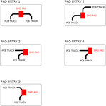
I also wanted to ask you: among the following PAD ENTRY options, which ones require a nail.

I think that option 1, 2, and 5 a nail is NOT required because the SMD PAD is not considered and end point by the CAM software.

What do you think of options 3 and 4?

PAD-ENTRY.jpg

> less test points is good. You reduce the time of testing
Could you be more specific on this issue?


Thank you for your opinion.

Enrico Migliore
 

Additionally, routing topology 2 is AFAIK better for EMC as it does not contain a spur.

Pad entry 1 is better for reflow as it balances the thermal cooling effect of the traces.


Or in other words, there is a heck of a lot more to routing a board than just considering the testing. :)
 

That is a very good point. Don't reduce test points if it will effect the quality of your pcb. On another note what type of pcbs do you guys lay out and what issue do you typically run into
When testing your designs? Just thought I would ask that questions. Do you guys design circuits that has a 75um(3mil) pitch or lower? I am interested to see why direction the pcb's are going? I work on applications where trace and spaces are 1mil/1mil. But these applications are development.
 

Interesting, in 25 years this is the first time I've seen this, I wouuld suspect you will have numerous more design considerations when laying out a PCB than how many bare board test points you have.
I worry about:
Signal Integrity
EMC
Power Delivery System
Board Assembly
I find that I do not have the time or the inclination to then fgo and try and reduce ATE testpoints!
Also good routing practice and signal integrity issues should give the optimum routing pattern, which generaly excludes branching etc.
An example is a simple board:) I'm playing with now, 100mm X 87mm, 3500 component pads, 1500 connections, if I started worrying about testpoints I go even more loopy than I already am:wink:

As to technology 0.075mm track, 0.1mm spacing is lowest I go to, anything below is getting into non-standard production for most (if not all) my suppliers, so you pay a lot more for your boards. I haven't had to go below the above mentioned sizes yet! but expect that as more and more BGA's apear with silly pitched (0.5mm and below) I may have to look at sub 0.075mm features.
 
  • Like
Reactions: taisen

    taisen

    Points: 2
    Helpful Answer Positive Rating
Hi folks,

I did quite a few EMC tests from 2001 up to now, and I can assure you guys that PAD entry doesn't influence EMC performances at all.

PAD entry may influence RF circuits performances at frequencies higher than 300 MHz.
For example, EDA softwares of RF circuits warn the RF designer about the parasitic capacitance that shows up between the two pieces of PCB track at 90 degrees:

|
|
|
|_________ PCB TRACK

EDA softwares will also suggest the RF designer how to modify the geometry of the miter in order to reduce the capacitance.


What metters in EMC is:

1) Current
2) Frequency
3) Loops Area

A sinusoidal current of 50 mA at 100 MHz that flows in a loop area of 100 mm^2 will create an Electric Field that exceeds the EMC residential limit, in Europe EN61000.
[Source: "EMC" video course produced by the Politechnic Institute of Turin - Italy]

Voltage doen't really metter. What metters is current.

In digital circuits we have peridic square wave currents and not sinusoidal waves currents.
In this case we have to do a Fourier analisys of the current and calculate the weight of the harmonics over the 300 MHz.

Enrico Migliore
 

Maybe everyone is going loopy then Marce :grin:

The last thing I usually worry about is the number of test points, you only pay for a test fixture the once.
It's not as if the text costs any more the higher the pin count.

In fact - many modern tests are flying probe -then there are only 2 pins.
 

Hi,

> many modern tests are flying probe
They are slower than traditional ATE machines.
They have the following advantages: they don't need fixtures (2000 $ saved) and don't need test points on the PCB.

> Interesting, in 25 years this is the first time I've seen this, I wouuld suspect you will have numerous more design
> considerations when laying out a PCB than how many bare board test points you have.
It's not a crime trying to reduce the number of end-points :)


Yet, nobody answered my question:

> I think that option 1, 2, and 5 a nail is NOT required because the SMD PAD is not considered and end point by the CAM software.
> What do you think of options 3 and 4?

Enrico Migliore
 

No its not a crime, but as I said I think there are much more important things to consider when doing a PCB, that are way more important. You are focusing on somthing that if you take all the other factors into consideration would be sorted out by the good design practice you would learn and develop. And the amount of money you would save would not be more than the amount of money it would cost to reduce the points, so why not concentrate on real PCB design issues and save money. Sorry changed my mind; yes it is a crime:lol:

Flying probe may be slower, but it also takes time to build a fixed point test jig, wire it up etc, and a fixed point is only useful for that issue of board, same thing happened with final electrical test. At one point every node was just about tested, now its boundry scan and/or functional block testing.

To answer your question, all pads have tracks going in and out so none are end points, but inermediate pads on a daisy chained signal.
 

Hi,

> there are much more important things to consider when doing a PCB, that are way more important
Those are already kept into account when I route a PCB.

> all pads have tracks going in and out so none are end points
Ok, thanks for your point of view.


> In fact - many modern tests are flying probe -then there are only 2 pins.
2 nails is the best case.
In some cases, you need 3 or 4 nails to measure the value of the component.


Enrico Migliore
 

According to my experience most of the fab houses have some what fixed tooling and testing costs.

some fab houses with online quote calculator doent ask for the files nor number of such test points.

AN example could be **broken link removed**
 

Status
Not open for further replies.

Part and Inventory Search

Welcome to EDABoard.com

Sponsor

Back
Top