kickoff1111
Newbie level 6
Hi all,
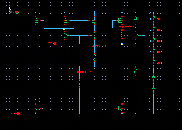
My bandgap circuit is as attached. With a start-up circuit using long channel length PMOS as resistive load and 2 diodes in series.
Now my wafers show low yield in VBG. Good dies show good distribution, but bad dies are all 0V.
Can anyone help me to figure out low yield is due to start-up circuit problem or process variation or others?
I have run all corners in transient and results are all OK, I don't know why.
Need your help.