Continue to Site

Welcome to EDAboard.com

Welcome to our site! EDAboard.com is an international Electronics Discussion Forum focused on EDA software, circuits, schematics, books, theory, papers, asic, pld, 8051, DSP, Network, RF, Analog Design, PCB, Service Manuals... and a whole lot more! To participate you need to register. Registration is free. Click here to register now.

Bandgap Startup circuit needed , with voltage limited devices

Status
Not open for further replies.

dominoeff

Junior Member level 1
Joined
May 6, 2010
Messages
17
Helped
0
Reputation
0
Reaction score
0
Trophy points
1,281
Location
china-mainland
Activity points
1,413
Hi Guys:
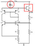
I am working on a bandgap circuit for a internal regulator in a DC-DC converter. The core circuit is a simple BROKAW bandgap circuit and i need a startup circuit for it.The problem is the input voltage is from 5~23 and the high voltage MOSFET my process provide have a max Gate-Source voltage(Vgs) of 5,while the max Base-Emitter(Vbe) voltage of 10.
Any suggestion or any paper reference is highly appreciated.

Thanks all.

Dominoeff
 

Hi Dominoeff
Without circuit topology, how you expect the startup circuit.
Start up circuit topology depends on the circuit architecture for which it has to be used. It helps to provide the path to create bias point.
Try to give some path which does not interfere your circuit operation.
 

Hi Dominoeff
Without circuit topology, how you expect the startup circuit.
Start up circuit topology depends on the circuit architecture for which it has to be used. It helps to provide the path to create bias point.
Try to give some path which does not interfere your circuit operation.
Thanks varunkant2k:
The core circuit is as below in core.png.I may change the BJT in red rectangle into a high voltage MOSFET.I also need a circuit to bias the current source in red ellipse.At first I want to use a BJT to mirror the current of Q3, and a P_MOSFET pair to mirror this current to get that current source . But when the input voltage is high , the gate-drain voltage (Vgs) of MOS or the BJT voltage (Vce or Vbe) will beyond the breakdown voltage. Later,I try a bipolar peak source to generate a current source and bias the circuit, it do not need a start up circuit but it need a big resistor and changed with the power supply(my input voltage range is large: 5v~23v).The worst thing is that I also find the BJT mirrors face the high voltage breakdown problem.

Dominoeff
 

Attachments

  • core.png
    core.png
    39.3 KB · Views: 149
Last edited:

In my process ,MOSFETs Vgs should be less than 5 ; BJTs Vbe should be less than 5 and Vce <10.
Dominoeff
 

hi Dominoeff, I did not get much in your writing. But Few questions I will try to suggest you.
Its better you provide constant voltage supply to band Gap circuit. You can try LDOs or Switching regulator.
Next for High Voltage supply, Why don't you go for cascode devices? using cacode Current mirrors helps you provide better load impedance.
VGs and VBE/VCE should not be problem once you use cascode device
 

In my process ,MOSFETs Vgs should be less than 5 ; BJTs Vbe should be less than 5 and Vce <10.
You didn't tell us about your current value (nor about your possible low power consumption requirement). So perhaps would it be possible to use a resistor + Z-diode regulation? For the Z-diode you could perhaps use the (reverse) Veb junction of a BJT.
 

Thanks varunkant2k and sorry for my poor writing.This band gap circuit is designed for my internal regulator to provide a reference voltage.The regulator , which is a LDO, will power my IC."Its better you provide constant voltage supply to band Gap circuit" does it mean i should use the output of my internal regulator(LDO) as the power supply of the bandgap? I use the input voltage to power my bandgap circuit because I think the reference voltage should be established first then the LDO can work correctly.Cascode devices will be a plus but i also need a structure workable.Thanks.
Dominoeff

---------- Post added at 03:11 ---------- Previous post was at 03:01 ----------

You didn't tell us about your current value (nor about your possible low power consumption requirement). So perhaps would it be possible to use a resistor + Z-diode regulation? For the Z-diode you could perhaps use the (reverse) Veb junction of a BJT.
Thanks erikl. It is ok if the current is under 25 micro.And the terrible process do not provide Z-diodes nor JFETs.
Dominoeff
 

I will prefer, to use constant Beta-multiplier for your LDO reference. It will be very tough for Band gap architecture to work on Sypply variation of from 5-23V. Better you provide less variation from basic LDO ( I prefer Swicthed regulator though) architecture using Constant Gm circuit. Then provide 5 volts +/- 500mV variation to Bandgap circuit. This should work fine.
 

I will prefer, to use constant Beta-multiplier for your LDO reference. It will be very tough for Band gap architecture to work on Sypply variation of from 5-23V. Better you provide less variation from basic LDO ( I prefer Swicthed regulator though) architecture using Constant Gm circuit. Then provide 5 volts +/- 500mV variation to Bandgap circuit. This should work fine.

Thank you, Varunkant2k.
I've consided many architectures including what you have provided. And the problem is my voltage limited devices .Many circuits are OK, if the input voltage is not high ( such as vin=5.5 ~10),but when the input goes higher , some of the MOSFETs or the BJTs will break down for their Vgs>5 or Vce>10. I try to find a way to protect my devices , which is inserting a High voltage MOSFET between the Vin and my bandgap circuit. I need a biasing circuit to bias the high voltage MOSFET and make sure their Vgs is always less than 5 , and this why i need some help about the start up circuits or bias circuits.
Dominoeff

---------- Post added at 09:22 ---------- Previous post was at 09:19 ----------

The correct input voltage Vin is 5.5~23, I've made a mistake.
 

Use clamper where you expect more than VGS/ VCE limit. One old Method I saw was, use diode connected devices across two biasing points. Where higher biasing point gets a path through low biasing point.
 

Use clamper where you expect more than VGS/ VCE limit. One old Method I saw was, use diode connected devices across two biasing points. Where higher biasing point gets a path through low biasing point.
Thanks.
And when the input voltage is 23, to protect the device i may need 3 or more serious diodes ,but they do not work when the input voltage is 5.5. What a terrilbe process!
 

Hi dominoeff!
I see that you are designing the startup circuit for LDO, i suggest that if your reference voltage is designing based on bandgap principle, the reference current should bias for some sub-block inside bandgap, and startup circuit you can use and array of NMOS is biased by current reference, then this array biasing for a mos that supply for the output stage of bandgap, then your circuit can start itself, also when the reference voltage is achieved, you should use an feedback mos to shut the bias for the Nmos array that i mentioned above <now, the bandgap can operate correctly itself>.

Hope this help!
 
  • Like
Reactions: butchi

    butchi

    Points: 2
    Helpful Answer Positive Rating
I will try these way later.
Thanks guys and Happy new year 2012.
Dominoeff
 

Status
Not open for further replies.

Part and Inventory Search

Welcome to EDABoard.com

Sponsor

Back
Top