Continue to Site

Welcome to EDAboard.com

Welcome to our site! EDAboard.com is an international Electronics Discussion Forum focused on EDA software, circuits, schematics, books, theory, papers, asic, pld, 8051, DSP, Network, RF, Analog Design, PCB, Service Manuals... and a whole lot more! To participate you need to register. Registration is free. Click here to register now.

Bad insersion loss coplanar waveguide

Status
Not open for further replies.

andiaye33

Newbie
Joined
Feb 19, 2021
Messages
3
Helped
0
Reputation
0
Reaction score
0
Trophy points
1
Activity points
53
Hello,

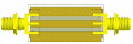
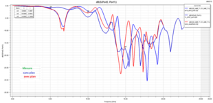
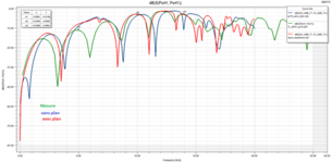
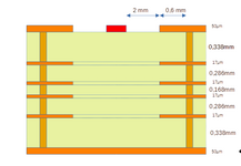
I’m simulation a Grounded CPW wint w=3.3mm, h=1.6 and g=2mm

in HFSS and getting invalid results near 10GHz.

Can someone help me please

Any suggestions are welcomed.
 

Attachments

  • ax70_v3_Light_b.rar
    69.8 KB · Views: 133
  • Image1.png
    Image1.png
    35.4 KB · Views: 236
  • Image3.png
    Image3.png
    62.8 KB · Views: 183
  • Image4.png
    Image4.png
    63.3 KB · Views: 199
  • stack.png
    stack.png
    35 KB · Views: 187
  • ANSYS_ax70.rar
    39.4 MB · Views: 142

What makes you think a multi layer board with stubs on the dual ground vias makes a good ground plane?
The coplanar tracks are OK but not the stubs orthogonal to the vias so near the dielectric between the conductors.
The Dk , low loss tangent , and etch back factors are also needed as well as type of gold plating.

it is also not drawn to scale and ought to have a w/h ratio near 2 depending on Dk or Er

For ~ 10 GHz you are concerned about zagged sharp edges for conductors and you have a comb running vertically on both sides producing lots of zeros.

1632447295091.png


The posts are high impedance on their own, so making the coplanar the same dimensions with stubs below is not good. This is a rough idea how to visualize the ground plane to scale.
 
Last edited:
Independent of the line itself, the gap in transition from connector to PCB creates series inductance.

serl.png


I had shown a similar testcase/example for simple GCPW with/without that gap here in the forum, the effect on return loss was impressive.

Line itself with coplanar ports:
model3d.PNG

gcpw_s2p.PNG


But the discontinuity from the coax transition damages response, by adding a lot of series L:
coax1.PNG

coax6_gaps.PNG

coax5_gaps.PNG
 
Last edited:
Good one Volker. Yes the pins and shoulder (I estimate) are about 0.5 nH/mm which is ~30 ohms per mm inductive @ 10 GHz with the gap having some capacitance in the cavity thus raising overall Z^2=L/C. It seems you chose around 3.8 for insulation.

Notice how Volker also made the coplanar distance much smaller than the inner post width. The ratios or conductor OD/ID determine the impedance in the coaxial get flattened into the rectangular wave guide . the coplanar insulation gap is not so sensitive as the vertical gap and conductor width. Since the skin effect is now about 0.6um (or about the 1/4 wavelength of UVC @ 10 GHz) the inner surface roughness in reality will also add length and inductance with scattering diffusion but not show up in your simulation.
 
Last edited:

    andiaye33

    Points: 2
    Helpful Answer Positive Rating
Thank you very much for your help sir SunnySkyguy and volker@muehlhaus.
I make the modifications in the simulations and I will come back to you for the new results
thank you
--- Updated ---

Independent of the line itself, the gap in transition from connector to PCB creates series inductance.

View attachment 172032

I had shown a similar testcase/example for simple GCPW with/without that gap here in the forum, the effect on return loss was impressive.

Line itself with coplanar ports:
View attachment 172036
View attachment 172037

But the discontinuity from the coax transition damages response, by adding a lot of series L:
View attachment 172038
View attachment 172039
View attachment 172042

Thank you for your help

I have change my simulation but i always see a bad insersion loss around 12Ghz
1632488785269.png


1632488819438.png


I think the problem come from via or internal plane
 

Attachments

  • stack.png
    stack.png
    35 KB · Views: 144
Last edited:

I would check the line itself by simulating without the SMA-models, using normal ports. That test tells you if the problem is in the line.

Your dimensions are quite large for that frequency, what is substrate permittivity? I would use a ground layer that is closer, to reduce line width.
 
Thank you for your reply, i used roger with er = 3.66
i have simulated the pcb alone but its complicated to know the return path without sma
 

With thinner substrate to gnd plane, you can achieve low impedance with thinner tracks and lower loss with less material in between.

But beware the dimensions become more critical with smaller size and electrical testing is recommended to validate Er with TDR supplier tests, while effective Er reduces with rising frequency in this range.

Z only depends on the surface ratios of the OD/ID for a given Er, and not so much the size.

However making a thin laminate makes it too flexible so a stiffener is needed underneath in some cases like bulk FR4 and surface roughness becomes more sensitive.

We used to make them in FPC this way for a flex cable to reduce flex but can be shaped.
 
Getting a high performance launch into a micro strip with side grounds and vias often is achieved with a combination of simulation and lab testing. I have often used Hittite and Southwest Microwave connectors and demonstration boards as a guide. The details of your particular connector and small gaps all play into the launch.

Typically the RF feed is on layer one and the ground plane is on the next layer. At 10 GHz a -15 to -20 dB s11 should be relatively easy to achieve and maintain. If your stack-up really puts the reference ground several layers down, that might be the source of your issue. Alternately, you could reduce the side gap spacing if you cannot put the ground on layer two but exciting the appropriate coplanar mode would be an issue. My preference is to keep the line looking like a simple micro strip with the strongest fields between the center conductor and lower ground.
 

Status
Not open for further replies.

Part and Inventory Search

Welcome to EDABoard.com

Sponsor

Back
Top