Continue to Site

Welcome to EDAboard.com

Welcome to our site! EDAboard.com is an international Electronics Discussion Forum focused on EDA software, circuits, schematics, books, theory, papers, asic, pld, 8051, DSP, Network, RF, Analog Design, PCB, Service Manuals... and a whole lot more! To participate you need to register. Registration is free. Click here to register now.

Avalanche Pulser

Status
Not open for further replies.

ghost896

Junior Member level 3
Joined
Jul 3, 2022
Messages
26
Helped
0
Reputation
0
Reaction score
0
Trophy points
1
Activity points
213
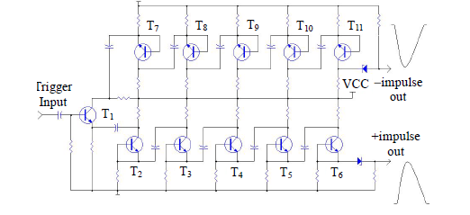
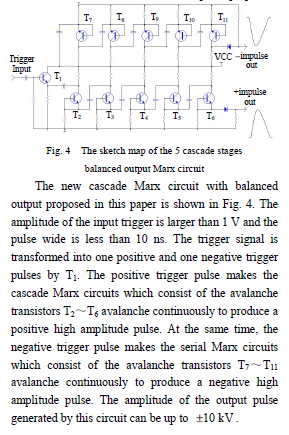
Hello everyone, I am researching on an avalanche based circuit with symmetric output. I have general information about avalanche transistors and how the marx generator works, but there are some parts that I do not understand in the circuit I shared.
The article mentioned that T1 changes the trigger voltage in positive and negative directions. I don't understand how this change happens. In this way, it puts the avalanche transistors in the upper and lower chains into avalanche mode.
Does anyone have a better explanation or understanding of the circuit?
1656868479230.png
1656868491474.png
 

Attachments

  • Design_of_Balanced_Output_High-Voltage_Nanosecond_.pdf
    492.1 KB · Views: 160

First, do you need the differential output? If you want a single-ended high voltage to ground, I think you should use a more "standard" Marx generator. The generator in this thread is only OK if you do a differential discharge between the output terminals.
Hello again thank you for your answer,
Yes, I want a differential output voltage and it's not critical that it's ground referenced, it's the potential difference that matters to me. I know of a product that gives this output, it gives a differential high voltage output with respect to ground and is made with the avalanche topology.

Before the trigger all capacitors and all transistors will have the VCC voltage across them.
They actually have fmmtd417 avalanche voltage ( 350V), not VCC voltage. Let's feed them with the voltage I want, they do not go over 350V. What exactly could be the reason for this?
--- Updated ---

When the trigger pulse comes, the potential of C3 (not the voltage across it) will increase and the potential of C2 will decrease.
Note : I had to remove the resistor R1 otherwise I can't get high voltage from the output.
I don't understand what you mean by C3 voltage. If you mean the T2 collector node voltage, when triggering, it drops from 350V to 160V and is charged back to 350V. The other pin of C3 is pulled to ground because I removed the resistor. As you said, C2 quickly discharges from 350V to 0V when the trigger comes.
--- Updated ---

This will increase the voltage across T2 and T7 to trigger the avalanche reaction, and this will lead to a chain reaction which causes the avalanche reaction in all transistors.
Exactly as you say, sir. Vce voltages rise a few volts above 350V and an avalanche occurs. I don't understand exactly how this voltage increase happens.
--- Updated ---

This casuses the strange jumps you see at T1. Every avalanche in the upper row of transistors will cause a positive jump in the potential of T1 (all 3 connections) and every avalanche in the lower row will cause a negative jump.
Yes I can see so clearly
--- Updated ---

The circuit is not very kind to T1. The emitter and collector will jump up and down, and the input capacitor will try to hold the base at a somewhat fixed potential. This will probably cause the avalanche to always happen first in the upper row of transistors, both in simulation and in a real circuit.
How can the T1 gate voltage go up to 30 volts? There is a current flow to the trigger source. Even if I put a diode in front of the source, there is a reverse current, it's really weird. I don't know if this will damage the resource. You also mentioned the gate capacitor, but even if I disable this capacitor, nothing changes, sir.
--- Updated ---

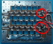
When I look at the pictures in the article referenced in post #1, it seems to be two transistors instead of only T1, one for each half of the circuit. That is probably a better solution.
When I look at the pictures in the article I see that there is only 1 trigger transistor in the middle.
 

The only explanation I have for positive jumps on T1 base is avalanche in T1. The current comes via C2.
I am not sure if the avalanche in T1 is intentional or a mistake.

The base-emitter junction of T1 has a much lower reverse voltage breakdown than collector to emitter or base,
so the base voltage can't deviate much from the emitter voltage.

It may be possible to trigger both halves at the same time without avalanche in T1, but the trigger voltage must then be much higher than 1V. Try 50-100V. R1 is needed for proper operation.

I don't like the circuit around T1. We can try to reverse engineer the dual transistor trigger circuit in the photo.
 
Status
Not open for further replies.

Similar threads

Part and Inventory Search

Welcome to EDABoard.com

Sponsor

Back
Top