Continue to Site

Welcome to EDAboard.com

Welcome to our site! EDAboard.com is an international Electronics Discussion Forum focused on EDA software, circuits, schematics, books, theory, papers, asic, pld, 8051, DSP, Network, RF, Analog Design, PCB, Service Manuals... and a whole lot more! To participate you need to register. Registration is free. Click here to register now.

Assura LVS issues with IBM 10LPE technology

Status
Not open for further replies.

rickgchen

Newbie level 6
Joined
Mar 28, 2011
Messages
12
Helped
0
Reputation
0
Reaction score
0
Trophy points
1,281
Activity points
1,510
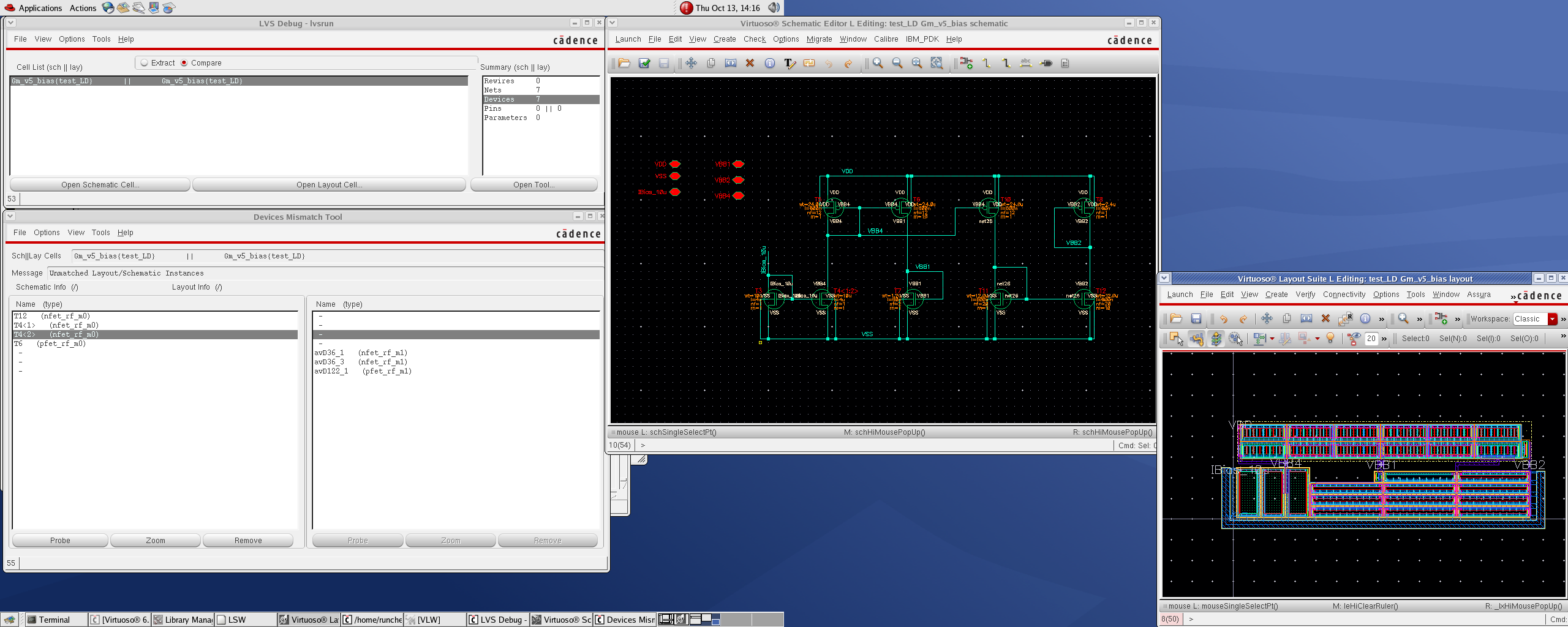
Hi everyone, I have a problem when doing Assura LVS checking. The PDK im using is IBM10LPE RF kit (05-01-00-01-LD). The problem is:

when doing Assura LVS cheking, there are two modes: CDL and VLDB.
(1) If I have device with multiplicity > 1, I have to generate CDL netlist and use LVS CDL mode. If I use VLDB mode, there will be error indicating multiplicity problems.
(2) If I have "ncap" device (it is a MOS varactor) in the schematic, when I use LVS CDL mode, the ncap device can not be matched. However, when I use VLDB mode, the ncap can be recognized.

In summary, if I have device with multiplicity > 1 without ncap, then LVS CDL mode works pretty well. When I have ncap device (maybe there are some other device too) without any multiplicity, LVS VLDB mode works well.

However, I have "ncap" and device with multiplicity > 1 in the same schematic, so how can I get LVS clean?

Thank you in advance.
 

(1) If I have device with multiplicity > 1, I have to generate CDL netlist and use LVS CDL mode. If I use VLDB mode, there will be error indicating multiplicity problems.

Yes this is in effect unfortunately,i encountered such a problem with IBM cms9flp last year...To avoid CDL netlisting and respective type of LVS
just use the bus naming instead of multiplicity at the properties of the device (for example for a fet T0 with desired m=2 write T0<0:1> or T0<1:2>).Then run VLDB LVS and will be clear.

(2) If I have "ncap" device (it is a MOS varactor) in the schematic, when I use LVS CDL mode, the ncap device can not be matched. However, when I use VLDB mode, the ncap can be recognized.

What kind of error do you get?Anyway,i suspect that aucdl view is missing for this device.You can see that from Library Manager.

Final conclusion : use my recommendations above and run VLDB,unless you know hot to create the aucdl view for the ncap if it is missing.
(it is quite easy,copy symbol view to a new view with name aucdl).
 
Hi jimito13,

Thanks for your reply. Actually I see your thread about this problem in Cadence forum. I tried to do bus name in VLDB mode but still get the LVS error. From the report, the schematic device is a bunch of device in parallel without merging, however, the layout extracted circtuit merged the device. So I still get the error using VLDB mode. Do you know how i should set up the switch or something to fix this problem.

For ncap device, i do have aucdl view. Are there any other possible problems?

Best,
 

Hi rickgchen,

Could you please upload a screenshot with the error when you try with bus naming?I can extract more info from this.Additionally the full LVS report would be even more descriptive.

Now as fas as the ncap it could be possibly a bug of this pdk...then you should report it to IBM.Although,have you read the manuals with the DRC,LVS,QRC guidance that exist it the path /tech_folder/IBM_PDK/cmos10lpe/Assura/doc?
Maybe there you can find a clue.
 
Hi Jimito13,

Here is a summary of the LVS report in VLDB mode. In the schematic, I changed one transistor with M=1 to be T4<1:2> like you said. In the LVS report, the schematic seems to treat the device as two seperate device while the layout part seems to combine them as a single device. There are two other transistors with M>1 which I did not change to bus mode, just to show you the LVS problems of this case.


Another good news I have, maybe I can share with you is, for the LVS CDL mode, the above problem does not exist. The only problem is it can not recognize the ncap device. I checked the netlist of ncap, it includes several parameters, e.g.

CC0 Cp Cn $[ncap] $SUB=sub! m=1 w=2u l=1u nf=10 nrep=2 mSwitch=0 composite=0

I understand the meaning of m, w, l, nf and nrep which are also physical device parameters. I dont understand the meaning of mSwitch and composite. If I change composite=0 to composite=1, then LVS get cleared in CDL mode. In order to pass LVS, I have to manually change this parameter in the netlist file generated by CDL. It seems to be a compromised solution but I dont know it is OK to do so.
 

In the schematic, I changed one transistor with M=1 to be T4<1:2>
Why you did this since device's m=1 initially.Maybe you meant this : Change from m=2 and T4 to m=1 and T4<1:2> ?

In the LVS report, the schematic seems to treat the device as two seperate device while the layout part seems to combine them as a single device
I don't think so,LVS report shows an 1-1 equivalence between sch. and lay. for this device but it seems that can't recognize them in layout and that's way there is a "-" there.
Try to delete the two instanses from layout and bring them back inside again so that they will take a correct naming.Maybe there is the problem.
I also noticed that you have net errors...can show them?Maybe there is something that triggers the devices errors.
The mystery is that you said with CDL is clean...do you mean it is clean with multiplicity m in CDL LVS and bus mode in VLDB LVS and that you showed the above image just to demonstrate the problem,so in above case if you
change the transistors with m to bus will pass LVS?Please clarify this case.

Now as for the composite parameter if i remember well from an old IBM's mail,it concerns the way that the device's parasitics are extracted...Did you read the manual i proposed you in a previous post?I think the answer is there as well for
the ncap LVS problem.Take a look there and come back if the problem still remains.
 
I tried to remove the old device in the layout and instantiate it again, now in schematic I am using bus mode instead of multiplicity and do LVS VLDB, it get cleared! Thank you for your hints.

If I still use LVS CDL, i need change the parameter of the ncap. I read all the PDK docs I have including the one you mentioned, there is nothing special mentioned about ncap or similar devices.

So now there are two ways to work out:

(1) Change multiplicity in schematic to bus mode + LVS VLDB.
This way I have to change the whole schematic, I have a big system and i just hate to do that.... :p

(2) Dont change the schmatic, just change one parameter in netlist file (ncap: composite = 1 -> 0) + LVS CDL.
It is much easier to do so since the deadline is very close. But not sure too much how this change affects the post-extraction (right now it seems ok).


Why you did this since device's m=1 initially.Maybe you meant this : Change from m=2 and T4 to m=1 and T4<1:2> ?

A typo. initially m>1.


I don't think so,LVS report shows an 1-1 equivalence between sch. and lay. for this device but it seems that can't recognize them in layout and that's way there is a "-" there.
Try to delete the two instanses from layout and bring them back inside again so that they will take a correct naming.Maybe there is the problem.
I also noticed that you have net errors...can show them?Maybe there is something that triggers the devices errors.
The mystery is that you said with CDL is clean...do you mean it is clean with multiplicity m in CDL LVS and bus mode in VLDB LVS and that you showed the above image just to demonstrate the problem,so in above case if you
change the transistors with m to bus will pass LVS?Please clarify this case.

Now as for the composite parameter if i remember well from an old IBM's mail,it concerns the way that the device's parasitics are extracted...Did you read the manual i proposed you in a previous post?I think the answer is there as well for
the ncap LVS problem.Take a look there and come back if the problem still remains.
 

Ok,i am glad that my suggestions helped you :)

Now as for the ncap,i prefer to be 100% sure about what i am doing when performing changes to the various devices' parameters.So,my recommendation is to create a simple test schematic with just one ncap and it's pins.Then run VLDB LVS without tweaking the composite option and write down the error,then send it to IBM and ask for more information and a final recommendation by them for the way you should treat this device.
 
Thanks for your help:)

I am writing a report to IBM about this issue.

Best,
 

Status
Not open for further replies.

Part and Inventory Search

Welcome to EDABoard.com

Sponsor

Back
Top