Arrowspace
Banned
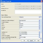
Hello, How can I calculate area of design hardware in xilinx
Follow along with the video below to see how to install our site as a web app on your home screen.
Note: This feature may not be available in some browsers.
par -filter iseconfig/filter.filter -w -intstyle ise -ol high -t 1
fir_4tap_map.ncd fir_4tap.ncd fir_4tap.pcf
Constraints file: fir_4tap.pcf.
Loading device for application Rf_Device from file '3s200a.nph' in environment C:\Xilinx\13.1\ISE_DS\ISE\.
"fir_4tap" is an NCD, version 3.2, device xa3s200a, package ftg256, speed -4
Initializing temperature to 100.000 Celsius. (default - Range: -40.000 to 100.000 Celsius)
Initializing voltage to 1.140 Volts. (default - Range: 1.140 to 1.260 Volts)
INFOar:282 - No user timing constraints were detected or you have set the option to ignore timing constraints ("par
-x"). Place and Route will run in "Performance Evaluation Mode" to automatically improve the performance of all
internal clocks in this design. Because there are not defined timing requirements, a timing score will not be
reported in the PAR report in this mode. The PAR timing summary will list the performance achieved for each clock.
Note: For the fastest runtime, set the effort level to "std". For best performance, set the effort level to "high".
Device speed data version: "PRODUCTION 1.41 2011-02-03".
Design Summary Report:
Number of External IOBs 25 out of 195 12%
Number of External Input IOBs 9
Number of External Input IBUFs 9
Number of External Output IOBs 16
Number of External Output IOBs 16
Number of External Bidir IOBs 0
Number of BUFGMUXs 1 out of 24 4%
Number of MULT18X18SIOs 1 out of 16 6%
Number of Slices 30 out of 1792 1%
Number of SLICEMs 1 out of 896 1%
Overall effort level (-ol): High
Placer effort level (-pl): High
Placer cost table entry (-t): 1
Router effort level (-rl): High
Starting initial Timing Analysis. REAL time: 8 secs
Finished initial Timing Analysis. REAL time: 8 secs
Starting Placer
Total REAL time at the beginning of Placer: 10 secs
Total CPU time at the beginning of Placer: 5 secs
Phase 1.1 Initial Placement Analysis
Phase 1.1 Initial Placement Analysis (Checksum:641) REAL time: 13 secs
Phase 2.7 Design Feasibility Check
Phase 2.7 Design Feasibility Check (Checksum:641) REAL time: 13 secs
Phase 3.31 Local Placement Optimization
Phase 3.31 Local Placement Optimization (Checksum:641) REAL time: 13 secs
Phase 4.2 Initial Clock and IO Placement
.........
Phase 4.2 Initial Clock and IO Placement (Checksum:fa01a56) REAL time: 21 secs
Phase 5.30 Global Clock Region Assignment
Phase 5.30 Global Clock Region Assignment (Checksum:fa01a56) REAL time: 21 secs
Phase 6.36 Local Placement Optimization
Phase 6.36 Local Placement Optimization (Checksum:fa01a56) REAL time: 21 secs
Phase 7.3 Local Placement Optimization
..........
Phase 7.3 Local Placement Optimization (Checksum:107998ff) REAL time: 25 secs
Phase 8.5 Local Placement Optimization
Phase 8.5 Local Placement Optimization (Checksum:107998ff) REAL time: 25 secs
Phase 9.8 Global Placement
..
..
Phase 9.8 Global Placement (Checksum:17bbf60e) REAL time: 25 secs
Phase 10.5 Local Placement Optimization
Phase 10.5 Local Placement Optimization (Checksum:17bbf60e) REAL time: 25 secs
Phase 11.18 Placement Optimization
Phase 11.18 Placement Optimization (Checksum:17b8802e) REAL time: 26 secs
Phase 12.5 Local Placement Optimization
Phase 12.5 Local Placement Optimization (Checksum:17b8802e) REAL time: 26 secs
Total REAL time to Placer completion: 26 secs
Total CPU time to Placer completion: 20 secs
Writing design to file fir_4tap.ncd
Starting Router
Phase 1 : 222 unrouted; REAL time: 30 secs
Phase 2 : 170 unrouted; REAL time: 30 secs
Phase 3 : 25 unrouted; REAL time: 30 secs
Phase 4 : 25 unrouted; (Par is working to improve performance) REAL time: 30 secs
Phase 5 : 0 unrouted; (Par is working to improve performance) REAL time: 30 secs
Updating file: fir_4tap.ncd with current fully routed design.
Phase 6 : 0 unrouted; (Par is working to improve performance) REAL time: 31 secs
Phase 7 : 0 unrouted; (Par is working to improve performance) REAL time: 31 secs
Updating file: fir_4tap.ncd with current fully routed design.
Phase 8 : 0 unrouted; (Par is working to improve performance) REAL time: 34 secs
Phase 9 : 0 unrouted; (Par is working to improve performance) REAL time: 34 secs
Phase 10 : 0 unrouted; (Par is working to improve performance) REAL time: 34 secs
Phase 11 : 0 unrouted; (Par is working to improve performance) REAL time: 34 secs
Phase 12 : 0 unrouted; (Par is working to improve performance) REAL time: 34 secs
Total REAL time to Router completion: 34 secs
Total CPU time to Router completion: 26 secs
Partition Implementation Status
-------------------------------
No Partitions were found in this design.
-------------------------------
Generating "PAR" statistics.
**************************
Generating Clock Report
**************************
+---------------------+--------------+------+------+------------+-------------+
| Clock Net | Resource |Locked|Fanout|Net Skew(ns)|Max Delay(ns)|
+---------------------+--------------+------+------+------------+-------------+
| Clk_BUFGP | BUFGMUX_X1Y0| No | 30 | 0.066 | 1.049 |
+---------------------+--------------+------+------+------------+-------------+
* Net Skew is the difference between the minimum and maximum routing
only delays for the net. Note this is different from Clock Skew which
is reported in TRCE timing report. Clock Skew is the difference between
the minimum and maximum path delays which includes logic delays.
Timing Score: 0 (Setup: 0, Hold: 0)
Asterisk (*) preceding a constraint indicates it was not met.
This may be due to a setup or hold violation.
----------------------------------------------------------------------------------------------------------
Constraint | Check | Worst Case | Best Case | Timing | Timing
| | Slack | Achievable | Errors | Score
----------------------------------------------------------------------------------------------------------
Autotimespec constraint for clock net Clk | SETUP | N/A| 4.399ns| N/A| 0
_BUFGP | HOLD | 1.619ns| | 0| 0
----------------------------------------------------------------------------------------------------------
All constraints were met.
INFO:Timing:2761 - N/A entries in the Constraints List may indicate that the
constraint is not analyzed due to the following: No paths covered by this
constraint; Other constraints intersect with this constraint; or This
constraint was disabled by a Path Tracing Control. Please run the Timespec
Interaction Report (TSI) via command line (trce tsi) or Timing Analyzer GUI.
Generating Pad Report.
All signals are completely routed.
Total REAL time to PAR completion: 39 secs
Total CPU time to PAR completion: 28 secs
Peak Memory Usage: 172 MB
Placement: Completed - No errors found.
Routing: Completed - No errors found.
Number of error messages: 0
Number of warning messages: 0
Number of info messages: 1
Writing design to file fir_4tap.ncd
PAR done!
With this information how can i calculate area required by my hardware ?