emaniac
Member level 1
Hi
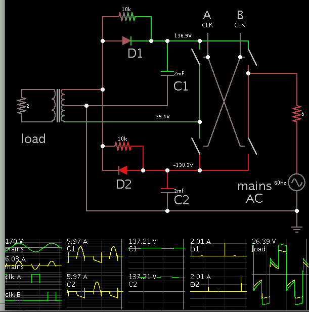
We have an Inverter Board that ceased working an year ago. It is a Push-Pull Converter Based one. The same circuit is used to charge the battery back from mains.
In the H- Bridge stage, It is IGBTs and not MOSFETs.

We have an Inverter Board that ceased working an year ago. It is a Push-Pull Converter Based one. The same circuit is used to charge the battery back from mains.
In the H- Bridge stage, It is IGBTs and not MOSFETs.