Continue to Site

Welcome to EDAboard.com

Welcome to our site! EDAboard.com is an international Electronics Discussion Forum focused on EDA software, circuits, schematics, books, theory, papers, asic, pld, 8051, DSP, Network, RF, Analog Design, PCB, Service Manuals... and a whole lot more! To participate you need to register. Registration is free. Click here to register now.

Analysing the LVDS CMFB feedback circuits

Status
Not open for further replies.

asuprash

Newbie level 6
Joined
Dec 6, 2006
Messages
11
Helped
1
Reputation
2
Reaction score
1
Trophy points
1,283
Activity points
1,371
Hi All,
I was trying to understand the CMFB circuit by for the LVDS by Boni.
From the circuit can somebody explain how the CMFB circuit works.

I have some more CMFB circuits that I am trying to understand.
This is the first one.

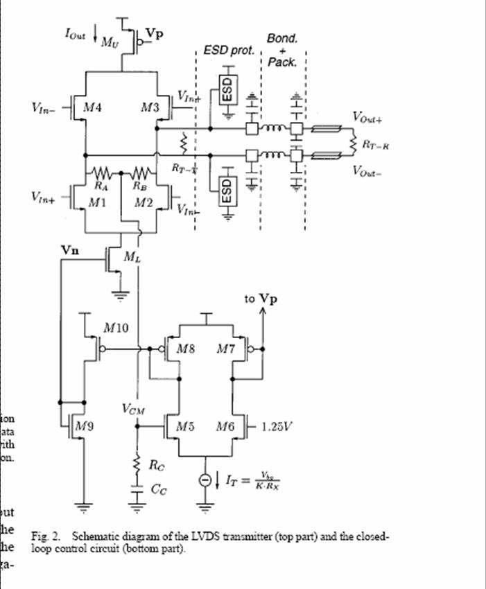
If Vcm increases above 1.25 V the current in the left leg increases
and the current in the right leg decreases.
The reduced current in the right leg causes an increase in Vp
This Vp being fedback to the LVDS transmitter causes a decrease in Iout, which
will inturn would cause an increase in the Common Mode voltage.

This would not appear to cause decrease in the CM voltage as expected.

Can anyone through light on the apparent ambiguity ?

Also, can some one explain the need for the pole-zero compensation that
is provided and how it benefits the circuit.

Regards Prashanth

58_1166506158.jpg


AA

Vcm increases, current in the left leg decreases , leads to decrease in the Vp, as we should need smaller Veff to pass smaller current with same W/L ratio, when Vp decreases, current Iout increases, which in turn decreases Vcm, as seen, it is a -ve feedback, about the R-C network, it is to compensate for the CMFB stability , it is inserted in the loop , so that it can compensate for stability , you can use cap. only if this enough to stabilize the circuit, if not enough , you might use R and C, you should first check the CMFB stability before adding the R-C network, and see if it is worth adding them
 

Vcm increase. the current in MU decrease, and the current in the ML increase. so the Vcm will decrease and the CMFB is functional.
 

    asuprash

    Points: 2
    Helpful Answer Positive Rating
Rewat,
U r wrong there... I was thinking about this and the correct explanation is:-

Vcm increases-> current in left leg increases -> current in right leg decreases->
Vp increases -> I(Out-Top) decreases

Vn increases-> I(Out-Bottom) increases

Since, I(Top) and I(Bottom) are now unbalanced Vcm has to fall to limit the flow
of current in the bottom tail transistor.

What I fail to understand now is -> Why do we have to give feedback to
the bottom tail source ? Why not bias it at a constant value ?
 
ravet said:
AA

Vcm increases, current in the left leg decreases , leads to decrease in the Vp, as we should need smaller Veff to pass smaller current with same W/L ratio, when Vp decreases, current Iout increases, which in turn decreases Vcm, as seen, it is a -ve feedback, about the R-C network, it is to compensate for the CMFB stability , it is inserted in the loop , so that it can compensate for stability , you can use cap. only if this enough to stabilize the circuit, if not enough , you might use R and C, you should first check the CMFB stability before adding the R-C network, and see if it is worth adding them

replace left leg with right leg, it is now true
 

How to simulate the cmfb performance in spice simulator ?
 

i also have same problem, may be u can break the loop for open loop gain plot, give ac input & check ac results at the ouput of feedback
 

Hi Prashanth,

This is in response to ur query, "What I fail to understand now is -> Why do we have to give feedback to the bottom tail source ? Why not bias it at a constant value ? "

My contention is that in the present case, wherein both both Vn and Vp are trying to control the value of Vcm, the -ve feedback will be more quicker than in the case wherein we may fix the value of the lower bias, Vn.

In case u find the argument specious, plz correct me. :)

Regards,
Vivek.
 

i agree with engrvivs's point.
there r 2 CMFB path, (1) is M5--> M7--> MU --> Vcm,
(2) is M5 --> M8 --> M10 --> M9 --> ML --> Vcm.
and path (1) should be slower than path (2), cuase MU has a high impedance load, while ML has a low impedance load.
using path (2) only is not a good idea, cause it maybe too slow to meet the spec.
 

yes vp will increase. two feedback paths helps to stabilize fastly.
 

It is a typical CMFB to stabilize the CM voltage level to the reference .
 

Status
Not open for further replies.

Similar threads

Part and Inventory Search

Welcome to EDABoard.com

Sponsor

Back
Top