Continue to Site

Welcome to EDAboard.com

Welcome to our site! EDAboard.com is an international Electronics Discussion Forum focused on EDA software, circuits, schematics, books, theory, papers, asic, pld, 8051, DSP, Network, RF, Analog Design, PCB, Service Manuals... and a whole lot more! To participate you need to register. Registration is free. Click here to register now.

Analog and digital switches/ maximum input signal frequency

Status
Not open for further replies.

sebas

Junior Member level 2
Joined
Oct 7, 2009
Messages
23
Helped
0
Reputation
0
Reaction score
0
Trophy points
1,281
Activity points
1,468
Hi,

Two beginner's questions:
1. What is the differences between an analog IC and a digital IC switch?
2. How can I find the maximum frequency for the input signal of a switch? I looked through the datasheet of a switch and I couldn't find a parameter that can tell me this. I want to use a switch to select between two clock sources.

Thanks!
 

For your case use a digital MUX (Multiplexer, aka Data selector) like, e.g. MC14051B (8 channels) or MC14519B (4*2 inputs / 4 outputs). Or 1 inverter and 2 NAND (or AND) gates.
 

That doesn't really answer my questions. Why are those circuits good?
 

Analog switches when turned on will conduct whatever voltage is on the input to the output pin. When turned off, the output is usually disconnected and floats at whatever voltage the surrounding circuit provides.
Digital switches when on, duplicate the logic level on the input pin at the output pin. Only logic levels are carried through the switch. When turned off, the output will assume a default logic state.

Analog switches have a frequency response that gradually reduces the output as the frequency increases beyond a certain point.
Digital switches have a maximum rate at which the output state will follow the input state, to calculate it, you need to look at the rise and fall times of the output and the delay between control signal changing and output enabling.


Brian.
 
  • Like
Reactions: sebas

    sebas

    Points: 2
    Helpful Answer Positive Rating
That doesn't really answer my questions.
This is true. However, I'm not prepared to answer general questions which can easily be answered by consulting any book about Electronic Design, or searching G00gle, Wiki, or this forum.

Why are those circuits good?
Because they'd fit for your application.
 

Analog switches when turned on will conduct whatever voltage is on the input to the output pin. When turned off, the output is usually disconnected and floats at whatever voltage the surrounding circuit provides.
Digital switches when on, duplicate the logic level on the input pin at the output pin. Only logic levels are carried through the switch. When turned off, the output will assume a default logic state.

Analog switches have a frequency response that gradually reduces the output as the frequency increases beyond a certain point.
Digital switches have a maximum rate at which the output state will follow the input state, to calculate it, you need to look at the rise and fall times of the output and the delay between control signal changing and output enabling.


Brian.

Hi,

Thanks for the reply. Any link to an article that discusses how to calculate the maximum rate?
 

I can't help with any articles but there are two factors to consider.

1. The output can't change faster than it's combined rise and fall time, these should be in the data sheet. The figures will probably be in nS and may vary according to the supply voltage and load conditions.
2. There will be a delay between the control signal (that activates the switch) changing and the output reacting to it. This is not related to the rise and fall time, it is more dependent on the internal delays in the control logic. the data sheet will normally specify this parameter too.

Brian.
 

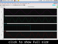
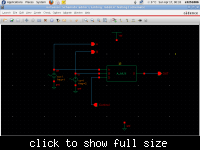
Hi all. I am having a similar question. I have two sine sources(1V-30Mhz and 1V-32Mhz). I wanna use an analog multiplexer to select between these two. The MUX i am using is based on this pdf www.fairchildsemi.com/ms/MS/MS-555.pdf.

However the output signal showed a big distortion. My question is how can I improve the output signal as much as possible.
I include here the circuit and the simulation waveform

Tks for any helps

---------- Post added at 15:43 ---------- Previous post was at 15:43 ----------


Answer to thanhFF´s problem:

You must put some load to mux output. (10k...470k resistor)
and look how output signal change.

Read this and try some mux ic in your circuit. (MAX4610 CD4066)

**broken link removed**


Regards KAK
 

Not thatway
I said "You must put some load to mux output."
So try 47k from out to ground
 

Does your simulated MUX handle positive and negative voltage swings?

Try adding resistors (try 10K) from A to ground and A to Vdd. Do the same for input B. this will raise the centre voltages of A and B so they do not swing below GND level.
Are you doing exactly what kak111 says, the load resistor goes between 'O' and Gnd, not in series with the output signal.

Brian.
 

Status
Not open for further replies.

Similar threads

Part and Inventory Search

Welcome to EDABoard.com

Sponsor

Back
Top