mvj
Advanced Member level 4
Dear All,
I am working on the layout of my circuit and I am having a problem which I am not able to resolve, can you please help me out.
When I run DRC I get the below mentioned error though the gate terminals are connected to a pin.
[1] ERCWarning: floating gate not connected to s/d, pad, pin or resistor.
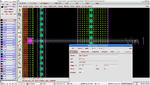
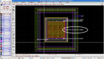
To reproduce this problem, i have taken a trasistor and connected pins to all the terminals of the device. At the gate terminal, I connected a poly to M1 contact, then VIA1, M2 Track and M2 pin (images attached for you reference). I have checked it throughly but I am not to resolve this problem. Can you please help me out.
Thanks a lot in advance!!
Best Regards,
M.
I am working on the layout of my circuit and I am having a problem which I am not able to resolve, can you please help me out.
When I run DRC I get the below mentioned error though the gate terminals are connected to a pin.
[1] ERCWarning: floating gate not connected to s/d, pad, pin or resistor.
To reproduce this problem, i have taken a trasistor and connected pins to all the terminals of the device. At the gate terminal, I connected a poly to M1 contact, then VIA1, M2 Track and M2 pin (images attached for you reference). I have checked it throughly but I am not to resolve this problem. Can you please help me out.
Thanks a lot in advance!!
Best Regards,
M.
 in; for example the latter is not exported to gds...