Continue to Site

Welcome to EDAboard.com

Welcome to our site! EDAboard.com is an international Electronics Discussion Forum focused on EDA software, circuits, schematics, books, theory, papers, asic, pld, 8051, DSP, Network, RF, Analog Design, PCB, Service Manuals... and a whole lot more! To participate you need to register. Registration is free. Click here to register now.

Amplifier question

Status
Not open for further replies.

boylesg

Advanced Member level 4
Joined
Jul 15, 2012
Messages
1,023
Helped
5
Reputation
10
Reaction score
6
Trophy points
1,318
Location
Epping, Victoria, Australia
Activity points
11,697
4TrAmp.gif


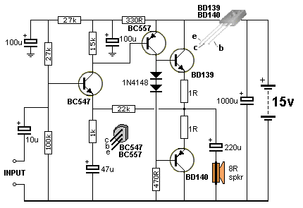
I have implemented this circuit on my bread board, but replaced the 1N4148 + 470R arrangment witha Vbe multiplier, and it seems to work OK with an ipod as audio input.

But I am running it of 12V instead of 15V. Are there any recommended changes for doing this?

The BD139 and BD140 seemed to get quite hot with the diode arrangement but I am able to 'dial' them down a little with my Vbe multiplier so that they dont get quite so hot.

I also made a seperate electret microphone pre-amplifier and AC coupled it to the above and it works really well.

- - - Updated - - -

Is the 470R the collector resistor for BC557?

And what are the 27k and 330r resistors about? I.E. The ones in series with Vcc.

I have a reasonable understanding of the rest of the circuit.

- - - Updated - - -

Perhaps one other thing. What are the two 1r resistors supposed to acheive?
 

Hi Boylesg


The BD139 and BD140 seemed to get quite hot with the diode arrangement but I am able to 'dial' them down a little with my Vbe multiplier so that they dont get quite so hot.
Rising the temperature when you don't have any input signal , is due to the improper DC bias of transistors .
But I am running it of 12V instead of 15V. Are there any recommended changes for doing this?
You should change your calculations of shut regulator ( BE shunt regulator ) .
( re design it with this value )
Is the 470R the collector resistor for BC557?
That resistor is used to bias the base of BD140 .
And what are the 27k and 330r resistors about? I.E. The ones in series with Vcc.
Such an arrangement has been called decoupling circuit to prevent bad effects of supply on behavior of your circuit .
Perhaps one other thing. What are the two 1r resistors supposed to acheive?
Those one ohm resistors are famous as temperature stability of your complement transistors .
Best Wishes
Goldsmith
 

Hi Boylesg
Rising the temperature when you don't have any input signal , is due to the improper DC bias of transistors .
Goldsmith
That is why I replaced the diodes with a Vbe multiplier, so that could ajust the bias.

Hi Boylesg
You should change your calculations of shut regulator ( BE shunt regulator ) .
( re design it with this value ) That resistor is used to bias the base of BD140 .
I would love to know how to do this Goldsmith. So you are talking about the 470R right?
Do you know of any websites that detail how you bias complementary piars? I have found plenty of websites detailing how you bias transistors as class A amplifier but none on how you bias complementary pairs with worked examples.


Such an arrangement has been called decoupling circuit to prevent bad effects of supply on behavior of your circuit .
Best Wishes
Goldsmith
Can you elaborate on what those bad effects might be?
 

The diodes/Vbe multiplier are to set the quiescent current of the output stage. With diodes, it's best to mount them on the heatsink with the output transistors so as they get warmer, the bias current is reduced to compensate. I'm not sure how you wired the Vbe Multiplier but if the voltage across it drops as it is heated, it should be used the same way on the heat sinks.

The idea is to overcome cross-over distortion by applying just enough bias on the output transistors that they start to conduct when there is no signal input (the 'A' in class 'AB'). Connect a current meter in the collector of one of the output transistors and check that the current is somewhere around the 5mA level WITH NO SIGNAL INPUT!. If it isn't, the Vbe multiplier isn't functioning properly. The current should increase as sound is produced and drop back tp quiescent level when the amplifier has no input again.

Brian.
 

Some circuit details don't seem to be well considered.

The 330 ohm/100 µF supply filter worsens noise suppression and should be better omitted.
The bias point should be adjusted for maximum undistorted output swing.
 

I would love to know how to do this Goldsmith. So you are talking about the 470R right?
Do you know of any websites that detail how you bias complementary piars? I have found plenty of websites detailing how you bias transistors as class A amplifier but none on how you bias complementary pairs with worked examples.
Hi Boylesg
You can find it in any textbook which deals with electronics basics . such as these books :
1-Practical electronics for inventors ( that's really awesome ) .
2- Fundamentals of micro electronics written by Behzad Razavi
3- Micro electronics by Jacob millman
4-Micro electronics by Adel Sedra
5- Electronic circuits and applications by irvin
6- ... etc .
or you can easily try to search it in google ! for example with these key words : how a class AB amplifier does work . or how to bias a class AB amplifier . or how a complementary amplifier does work or anything else like this .
Can you elaborate on what those bad effects might be?
Of course
You have two sections in each amplifier in this world !! first section is low power section and the other section is high power stage .
As you probably know each high power stage will require large value of current . and again as you probably know each PCB line , has an equivalent circuit which can be modeled with RLC circuits !
And as i hope you know , when your power stage is working , the voltage across the PCB line will have large variations . these variations can suffer or destruct the behavior of low power stages because the minimum variations in a low power stage can change it's quiescent point and then it can destroy behavior of it and it will make it unstable . hence such a filter will be required which usually called " Decoupling circuit" .
What can do this circuit or what is the profit of such a network ? in fact a capacitor will be charged till supply voltage and then the low power stage won't get it's required current , directly from the main power line ! it will take it's required current from that capacitor !! now i can guess , you'll ask why we used that resistor before that capacitor ? the answer is simple ! because the power stage will require large amount of surge current ! and then that resistor has a large value instead of that current and it can't take it's required current from that capacitor ! hence it can't discharge that capacitor ! hence just the low power stage can take current from that capacitor !
You understand my descriptions ?
Best Wishes + Good Luck
Goldsmith
 

Hi Boylesg
You can find it in any textbook which deals with electronics basics . such as these books :
1-Practical electronics for inventors ( that's really awesome ) .
2- Fundamentals of micro electronics written by Behzad Razavi
3- Micro electronics by Jacob millman
4-Micro electronics by Adel Sedra
5- Electronic circuits and applications by irvin
6- ... etc .
or you can easily try to search it in google ! for example with these key words : how a class AB amplifier does work . or how to bias a class AB amplifier . or how a complementary amplifier does work or anything else like this .

Of course
You have two sections in each amplifier in this world !! first section is low power section and the other section is high power stage .
As you probably know each high power stage will require large value of current . and again as you probably know each PCB line , has an equivalent circuit which can be modeled with RLC circuits !
And as i hope you know , when your power stage is working , the voltage across the PCB line will have large variations . these variations can suffer or destruct the behavior of low power stages because the minimum variations in a low power stage can change it's quiescent point and then it can destroy behavior of it and it will make it unstable . hence such a filter will be required which usually called " Decoupling circuit" .
What can do this circuit or what is the profit of such a network ? in fact a capacitor will be charged till supply voltage and then the low power stage won't get it's required current , directly from the main power line ! it will take it's required current from that capacitor !! now i can guess , you'll ask why we used that resistor before that capacitor ? the answer is simple ! because the power stage will require large amount of surge current ! and then that resistor has a large value instead of that current and it can't take it's required current from that capacitor ! hence it can't discharge that capacitor ! hence just the low power stage can take current from that capacitor !
You understand my descriptions ?
Best Wishes + Good Luck
Goldsmith

"the minimum variations in a low power stage can change it's quiescent point "

A little confused by this - you have inadvertently worded this in a fairly ambiguous way as I read it.


Variations in the lower power stage can change the quiescent current of the high power stage or large variations in the high power stage can change the quiescent current of the lower power stage?

I would assume the latter.

If the latter then I can begin to understand why you need negative feed back from the higher power stage back to the lower power stage.

Correct me if I am wrong.

This seems to generally take the form of R1 in the base voltage divider of the lower power stage being connected to the emitters of the high power complementary pair stage (in class AB amplifiers) rather than to Vcc.

So the fact that the voltage divider at the base of the low power stage is always being fed by a variable rather than fixed voltage source is clearly going to effect its quiescent current. But I still can't get my head around how it this prevents run away and distortion.

The resistors in the voltage dividers are nearly always large value ones so only a small amount of the current from the high power complementary stage will feed back to the low power stage

From what you have said, if you were to AC couple rather than DC the lower power stage and the high power stage, then you would not need negative feedback?
But what are the disadvantages of doing this given that there are few if any examples of people doing this?


The signal at the high power stage would not be exactly in phas with

- - - Updated - - -

I have read "The art of electronics" and a few other books but none get into the nitty gritty of example biasing a complemtary pair and seem to confine themselves to the general theory of how they work.

I will see if I can find some copies of the books you have listed at our local library.

- - - Updated - - -

"Practical electronics for inventors"

I believe I have found this as an ebook (pdf): http://www.studio250.fr/docs/divers%20trucs/Practicl%20Electroncsnventors.pdf
 

A little confused by this - you have inadvertently worded this in a fairly ambiguous way as I read it.
Hi Boylesg
What i've told before ? think about tracks of your PCB as an RCL filter ! each audio amplifier works in gang of audio frequencies ! and then think about effects of such a filter instead of a DC current which has variations according to the audio signal ! when current is high ( for power stage ) then variations will be higher and such an effect will appear larger . so VCC of low power stage will have variations ! then it will be cause of bad voices and noises in your speaker .
If the latter then I can begin to understand why you need negative feed back from the higher power stage back to the lower power stage.
Negative feedback isn't necessary for every circuit ! it depends on the designer . basically negative feedback can change these parameters :
1-Band Width (BW)
2- input and out put impedances
3- Current gain
4- voltage gain
5- Linearity and non linearity of your amplifier ( it has direct effect on THD ) (i.e : THD = Total harmonic distortion )
( but changing in those parameters depends on what kind of negative feed back has been applied in design ! for example in your circuit the feed back is series voltage )
m of R1 in the base
I think you're referring to the 27 K ohms resistor of base of bc547 ?
On he other hands negative feedback has gang of advantages . but in simple words it will help your amplifier to be more stable and it will also deliver lower THD .
amplifiers) rather than to Vcc.

So the fact that the voltage divider at the base of the low power stage is always being fed by a variable rather than fixed voltage source is clearly going to effect its quiescent current. But I still can't get my head around how it this prevents run away and distortion.

The resistors in the voltage dividers are nearly always large value ones so only a small amount of the current from the high power complementary stage will feed back to the low power stage
A question : Did you ever read any text book about Class A and AB amplifiers ? for example do you know what is the action of base bias resistors of first stage ? if we change value of them , what will change in your circuit ? do you know these things ?
d the high power stage, then you would not need negative feedback?
You should understand concept of negative feedback and it's duty . consider , that you have two ears . when you are talking to someone , you can hear your own voice too and then control value of your sound . just put your hands on your ears . and try to talk to someone ! what will happen ? you'll increase amplitude of your sound ! why ? to be able to hear it ! but your friend ( the person who has conversation with you ) will tell you , why you are increasing your voice !! your voice is suffering me ! so what happened ? your ear has another duty ! negative feedback ! when you want to talk to someone . it will aid you to control your voice . if you being in a noisy place you will try to increase your sound and when you go to the calm places such as library , you'll try to decrease your voice . why ? because that place is very calm and you can easily hear your own voice .

Appraisal :
A negative feed back will control many things in a circuit ! ( and also in everything ! ) .

Best Wishes + Good Luck
Goldsmith
 

Hi Boylesg
What i've told before ? think about tracks of your PCB as an RCL filter ! each audio amplifier works in gang of audio frequencies ! and then think about effects of such a filter instead of a DC current which has variations according to the audio signal ! when current is high ( for power stage ) then variations will be higher and such an effect will appear larger . so VCC of low power stage will have variations ! then it will be cause of bad voices and noises in your speaker .

Negative feedback isn't necessary for every circuit ! it depends on the designer . basically negative feedback can change these parameters :
1-Band Width (BW)
2- input and out put impedances
3- Current gain
4- voltage gain
5- Linearity and non linearity of your amplifier ( it has direct effect on THD ) (i.e : THD = Total harmonic distortion )
( but changing in those parameters depends on what kind of negative feed back has been applied in design ! for example in your circuit the feed back is series voltage )

I think you're referring to the 27 K ohms resistor of base of bc547 ?
On he other hands negative feedback has gang of advantages . but in simple words it will help your amplifier to be more stable and it will also deliver lower THD .

A question : Did you ever read any text book about Class A and AB amplifiers ? for example do you know what is the action of base bias resistors of first stage ? if we change value of them , what will change in your circuit ? do you know these things ?

You should understand concept of negative feedback and it's duty . consider , that you have two ears . when you are talking to someone , you can hear your own voice too and then control value of your sound . just put your hands on your ears . and try to talk to someone ! what will happen ? you'll increase amplitude of your sound ! why ? to be able to hear it ! but your friend ( the person who has conversation with you ) will tell you , why you are increasing your voice !! your voice is suffering me ! so what happened ? your ear has another duty ! negative feedback ! when you want to talk to someone . it will aid you to control your voice . if you being in a noisy place you will try to increase your sound and when you go to the calm places such as library , you'll try to decrease your voice . why ? because that place is very calm and you can easily hear your own voice .

Appraisal :
A negative feed back will control many things in a circuit ! ( and also in everything ! ) .

Best Wishes + Good Luck
Goldsmith

The voice analogy re feedback was rather helpful. I take it then that, although it is called negative feedback, it is not always entirely negative. I.E. It could be more negative or less negative depending on the conditions in the power stage.

A question : Did you ever read any text book about Class A and AB amplifiers ? for example do you know what is the action of base bias resistors of first stage ? if we change value of them , what will change in your circuit ? do you know these things ?

As I understand at present the voltage divider on the base is designed to set the base at a voltage such that the required quiescent base current will flow through the BE junction given that it has some resistance while operating in its active region.......V=IR and all that.

I am really trying hard to understand this stuff but I am doing so from a quite low base....be patient with me.

I have been reading any and material on the web I can find and, with help from you guys, very slowly my understanding is improving.
 

I am really trying hard to understand this stuff but I am doing so from a quite low base....be patient with me.

I have been reading any and material on the web I can find and, with help from you guys, very slowly my understanding is improving.
No problem . i'm so patient in teaching ! :wink:

Now is your problem solved ?
Best Wishes
Goldsmith
 

No problem . i'm so patient in teaching ! :wink:

Now is your problem solved ?
Best Wishes
Goldsmith

If the following is a correct interpretation then my problem is well on the way to being solved:

As I understand at present the voltage divider on the base is designed to set the base at a voltage such that the required quiescent base current will flow through the BE junction given that it has some resistance.......V=IR and all that.

I still probably have a little way yet to go before I have complete confidence in designing a class A amplfier on my own.

With the help of that transistoramp software, I have been varying the voltage gain, input impedance and output impedance and observing the effect this has on resistor values.

So this software has improved my understanding of the biasing as well.
 

Status
Not open for further replies.

Part and Inventory Search

Welcome to EDABoard.com

Sponsor

Back
Top