ChetanGK
Newbie level 6
Hi all,
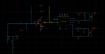
I am designing a front end for capacitive sensing application and mixer for lock-in demodulation. The mixer is double balanced voltage mode passive mixer (50% duty cycle) and LPF filter is differential RC filter for cut off frequency of 1KHz. Please find the attached image(system.png)
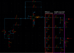
One of the mixer input is connected to amplifier output and the other input of the mixer is connected to reference voltage. The mixer's differential output is connected to differential RC LPF. The equivalent circuit (not sure though) can be seen from image (equivalent_load.png).
I am at stage of decide the second stage topology for my front end amplifier. As it is not typical capacitive load, I am not sure about what topology fits my application.
Amplifier specification(preliminary)
GBW ~ 400Mhz (based on Noise gain)
F3db = 20MHz (closed loop)
Noise gain ~ 15 (Cf = 60f , differential sensor cap = 700f )
Acl = 0.5
Aol = 65dB
Can someone please guide how to analyse the load for the amplifier and topology for second stage?
Thanks in advance
Regards,
Chetan
I am designing a front end for capacitive sensing application and mixer for lock-in demodulation. The mixer is double balanced voltage mode passive mixer (50% duty cycle) and LPF filter is differential RC filter for cut off frequency of 1KHz. Please find the attached image(system.png)
One of the mixer input is connected to amplifier output and the other input of the mixer is connected to reference voltage. The mixer's differential output is connected to differential RC LPF. The equivalent circuit (not sure though) can be seen from image (equivalent_load.png).
I am at stage of decide the second stage topology for my front end amplifier. As it is not typical capacitive load, I am not sure about what topology fits my application.
Amplifier specification(preliminary)
GBW ~ 400Mhz (based on Noise gain)
F3db = 20MHz (closed loop)
Noise gain ~ 15 (Cf = 60f , differential sensor cap = 700f )
Acl = 0.5
Aol = 65dB
Can someone please guide how to analyse the load for the amplifier and topology for second stage?
Thanks in advance
Regards,
Chetan