samson41879
Newbie level 2
Hello people from snowy Zagreb, Croatia. This is my first post here. Great community - keep going...
I have some questions regarding custom footprint design in Altium Designer 10.
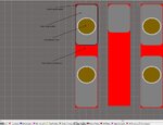
You will find below a picture of FAKRA high speed connector footprint. I made the picture in Top Paste layer just for you to see where are the pads which are on a top layer.
1. Solder paste has to be printed into vias as well as on the pads. How I define that in Altium Designer?
2. Can I put the pads on the copper fill or pads have to be extensions of the copper fill?
3. Do you have some other advices or you see that I am doing something wrong based on the recommended footprint from the datasheet (see above link)?
Thank you very much for your time!
Best Regards!
