Continue to Site

Welcome to EDAboard.com

Welcome to our site! EDAboard.com is an international Electronics Discussion Forum focused on EDA software, circuits, schematics, books, theory, papers, asic, pld, 8051, DSP, Network, RF, Analog Design, PCB, Service Manuals... and a whole lot more! To participate you need to register. Registration is free. Click here to register now.

Altium designer Questions

Status
Not open for further replies.

elec-eng

Full Member level 5
Joined
Nov 16, 2006
Messages
243
Helped
20
Reputation
40
Reaction score
5
Trophy points
1,298
Activity points
2,927
autoplacer

I have four questions about Altium designer 6.6

Q1)i have proben with Auto route

When i droaw a schematic and compile it successfully without any errors then i update it to a pcb and when i perform auto route the software dont route all connections and it partially route the pcb
like this

3_1183924789.jpg


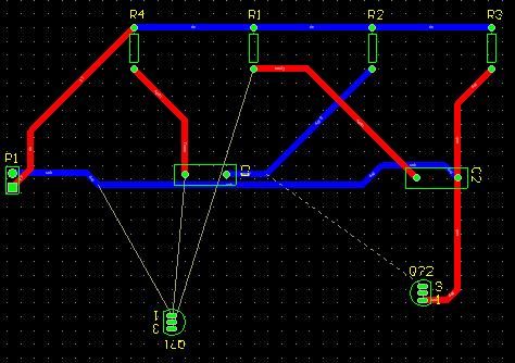
So how to solve this problem and make the software performs complete auto rote process


Q2) is there a method to make the software auto places the components on pcb for best routing since i had to place the components manually in their possitions


Q3)How to make a single layer for simple designs like this shown in the previous image since Altium automatically route it as two layers although it is very simple!


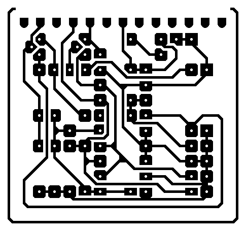
Q4)How to produce such this image from a pcb using Altium


60_1183925143.gif


Thank you very much
 

printing 1:1 altium

Q1)i have proben with Auto route

A1) looking at the picture there may be few things that can effect it, 1 os the clearance rule, 2, the witdh rule and how you got to set it up for auto route aslo how your compents are palced.

Q2) is there a method to make the software auto places the components on pcb for best routing since i had to place the components manually in their possitions

a2 your best bet is to place them manualy I found that the autoplacer is no good, the way I do it is print of the schematic than place them logically according to your schematic i.e place say IC1 then R1 around IC1 an so on.


Q3)How to make a single layer for simple designs like this shown in the previous image since @ltium automatically route it as two layers although it is very simple!

A3. I have uploaed a short video to show you how it is easier to do it that way

Q4)How to produce such this image from a pcb using @ltium

A4. I use a PDF print engine (adode acbrobat 8) ad all ways get 1:1 size,
What I will do is another simple video to show you how


wizpic
 

    elec-eng

    Points: 2
    Helpful Answer Positive Rating
altium autoplacer

thank you

but i cant see the attachment to download

please send me its link

thanks
 

here are they are again
 

    elec-eng

    Points: 2
    Helpful Answer Positive Rating
it is there I cna see it now

Added after 22 minutes:

sorry I just checked them and I can see nothing when i unziped them but these 2 file work now
 

    elec-eng

    Points: 2
    Helpful Answer Positive Rating
@ltium designer Questions

elec-eng did this help you ?

If need be I can do more mini tuts if anybody wants to know and i will see if I can do it.

Added after 50 minutes:

elec-eng
I think I understand what you want to do in your PM
There are 2 way you can use polyigon or solid fill so you have less area to eacth away

I'll sort it out
 

    elec-eng

    Points: 2
    Helpful Answer Positive Rating
@ltium designer Questions

Thank you very much
 
elec-eng
go here and you will find all the information you need it's the tranning manuals for altium, I did the videos beacuse they are easier than typing how to do it, But i have lack of time on my hands at the moment I have a big contract to finish off


https://www.altium.com/Community/Support/TrainingManuals/

hope this helps you, a little reading never hurt anybody

wizpic
 

Here is the polyigon (copper fill) video if you still need it

anymore questions just ask away
 

Status
Not open for further replies.

Part and Inventory Search

Welcome to EDABoard.com

Sponsor

Back
Top