Continue to Site

Welcome to EDAboard.com

Welcome to our site! EDAboard.com is an international Electronics Discussion Forum focused on EDA software, circuits, schematics, books, theory, papers, asic, pld, 8051, DSP, Network, RF, Analog Design, PCB, Service Manuals... and a whole lot more! To participate you need to register. Registration is free. Click here to register now.

Altium designer: How to assign a filled region to a pin of footprint in PCB library

Status
Not open for further replies.

rehakm

Junior Member level 1
Joined
May 31, 2011
Messages
15
Helped
1
Reputation
2
Reaction score
1
Trophy points
1,283
Activity points
1,421
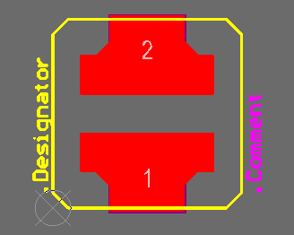
I have some footprints with non-trivial pads. I used a region in top layer over a pin to model required shape. How do I assign this region to overlayed pin? I can see there's Net option in pin and region properties but cannot choose nothing (not surprised in library where no nets).
The problem is after placement this footprint in PCB editor and running DRC - it reports me short circuit violation between the region and pad. I'm unable to get region properties dialog probably because it's part of a footprint.
In OrCAD Layout there's an option for obstacle "Assign to pin" that do this. Maybe other option would be draw a special polygonal pad but I don't see it in Altium.

92_1307554760.png
 

Another former OrCAD user here :)
Yes, this kind of complex pads cannot be freely implemented by adding of regions - I have tried that and failed. If 45deg corners doesn't matter you can try to combine a complex pad by 2 ones with the same designator. Good luck!
 

Another former OrCAD user here :)
Yes, for about ~5 years of work... :)
Now I'm learning Altium. Currently my opinion is that it is more complex and better system but some operations cannot be done as quickly as in OrCAD by one key (if I'm not going to write a script) and maybe some cannot be done at all?

Yes, this kind of complex pads cannot be freely implemented by adding of regions - I have tried that and failed. If 45deg corners doesn't matter you can try to combine a complex pad by 2 ones with the same designator. Good luck!

Hm, it sounds like dirty H4CK :\ Hope there's better option that only remained hidden to us :)
 

Yes, for about ~5 years of work... :)
Now I'm learning Altium. Currently my opinion is that it is more complex and better system but some operations cannot be done as quickly as in OrCAD by one key (if I'm not going to write a script) and maybe some cannot be done at all?

It's a common opinion for all who just started to use AD. In fact this product is very convenient and much more powerful than your beloved OrCAD. Just take your time. If you have lost or just a doubt in your mind there is always a person who'll give a hand.
 

the command you are looking for is called "update free primitives from component pads" on the pcb side.
look under >>design >> netlist >> update free primitives from component pads.
 
Thank u loosemoose - I knew something should be possible!
 

the command you are looking for is called "update free primitives from component pads" on the pcb side.
look under >>design >> netlist >> update free primitives from component pads.

Thakn you, it works fine. I expect that when I add another such component in PCB I'll have to do this again to update new region.

>androm
I never said "beloved OrCAD", I know about some anying bugs that was not fixed from v.9.3 to 16.3 that I worked on but I learned to live with it...
 

Status
Not open for further replies.

Part and Inventory Search

Welcome to EDABoard.com

Sponsor

Back
Top