Continue to Site

Welcome to EDAboard.com

Welcome to our site! EDAboard.com is an international Electronics Discussion Forum focused on EDA software, circuits, schematics, books, theory, papers, asic, pld, 8051, DSP, Network, RF, Analog Design, PCB, Service Manuals... and a whole lot more! To participate you need to register. Registration is free. Click here to register now.

Altium Designer - Edit Full Pad for single layer pads

Status
Not open for further replies.

cosyne

Newbie level 3
Joined
Aug 17, 2008
Messages
3
Helped
0
Reputation
0
Reaction score
0
Trophy points
1,281
Activity points
1,302
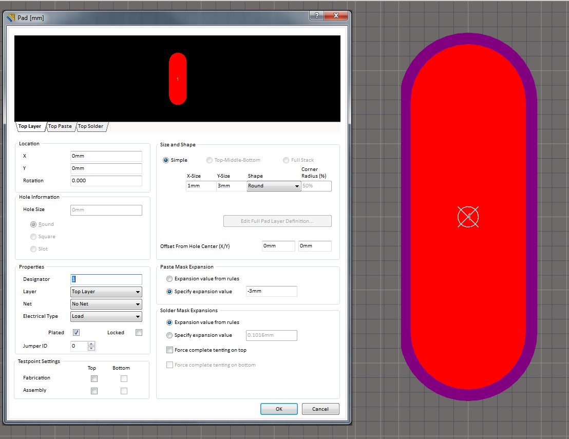
I can not find how to edit single layer pads.
For single layer pads, the “Edit Full Pad Layer Definition …” button is inactive.

I need single layer pads not covered by solder paste, or AD 10 automatically assigns the aperture for solder paste layer and I only could change the expansion value for solder paste layer aperture but I can not completely remove that aperture.
 

you can add a negative size to the solder mask expansion, usually half the pad size.
If you have a newer version you can enable "force complete tenting option".
 

Thank you loosemoose.

I tryed negative size to the solder mask expansion but it doesn't work, I still have apertures generated in solder paste layer.
I can not force complete tenting because I don't want pads covered by solder mask either, I want to have the gold finish from the manufacturer on them. It's about an edge connector for like a SIMM 72 form PCB
 

cosyne - Did you ever find a solution for this ? I have the same situation, I need several large top-layer pads for direct wire-bonding. I want solder mask in place, but NO paste openings.

-pana
 

Hi panalog9,

I did not found a solution in Altium and as far as I can see it working I don't think there is a solution in this release level.

What I did: I edited the gerbers in a gerber tool (Visual CAM ) and did the modifications directly on gerbers.

Hope this helps you.
 

Hi Guys,

loosemoose is right although you were talking about paste and he talking about mask... Check out the screen shot I've got my paste mask expansion set to -3mm and the view of the pad is shown from the top paste there would be a grey colour on it if it was covered with solder paste the purple is the solder mask in negative.


It may be a little late but I hope this helps.
Chris.
 

Status
Not open for further replies.

Part and Inventory Search

Welcome to EDABoard.com

Sponsor

Back
Top