Continue to Site

Welcome to EDAboard.com

Welcome to our site! EDAboard.com is an international Electronics Discussion Forum focused on EDA software, circuits, schematics, books, theory, papers, asic, pld, 8051, DSP, Network, RF, Analog Design, PCB, Service Manuals... and a whole lot more! To participate you need to register. Registration is free. Click here to register now.

Altium design - avoiding polygon pours over No Net pads

Status
Not open for further replies.

toni.bb

Newbie level 3
Joined
Nov 15, 2010
Messages
3
Helped
0
Reputation
0
Reaction score
0
Trophy points
1,281
Activity points
1,313
Hi all,
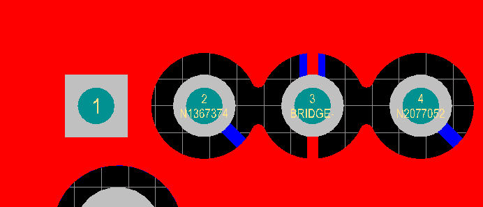
I have created a Polygon Pour in Altium Designer. The issue is that it pours over components' pads that are not connected to any net. I don't want this behaviour, but after searching and reading several docs/posts I haven't yet found the way of avoiding this. I know that electrically there is no problem, but I would like that the Pour avoids the pads that are assigned to "No Net" (for easiness of soldering).

Some properties of the created Polygon Pour are:
- Connect to Net: "No Net"
- and "Don't Pour Over Same Net Objects"
(I think these are the most relevant properties with relation to this question)

I will appreciate any help with this issue.

Thanks in advance!

Toni
 

Hi,

I think the problem lies with in the Polygon. You have not connected the polygon to any connection..
if you really want to have a dead polygon (connected to NO Net). Select the option "Pour over same Net polygons only". this would solve the issue.
 

Thanks for your reply.
However, I tried the option "Pour over same Net polygons only" with no success. The polygon still pours over the "No Net" pads.

Anyway, I think that the problem is not related to the fact that the polygon is not connected to any net. I've changed it in order to connect to a GND net, and then the polygon connects with thermal reliefs to GND pads, but connects covering completely the "no net" pads.

---------- Post added at 16:03 ---------- Previous post was at 15:59 ----------

I attach a picture showing what happens.
For instance, I connect the polygon to a ground net (named "BRIDGE-"). In the picture you can see a "BRIDGE-" pad (pin 3) with thermals, and a "no net" pad (pin 1) completely flooded by the polygon, which is what I try to avoid.


It will connect to "no net" pads as you are assigning a net name (as altium sees it), it is similar to assigning any other net name, as you have tried with GND, and if you leave the net name option empty it wont pour any copper.
I think you want to put dead copper on PCB for PCB balancing.One option I think for this is you can provide "Solid region" rather than Polygon pour but it has to be only at empty places otherwise it will show error.
This very cumbersome but I guess would be effective or check if there is any option for "Cu balance"or "thieving" in Altium.
 

verify your design rules settings, if no net pads are ignored some how

Your suggestion was crutial!! :-D
The issue was that I wanted to have a different clearance between traces than between pours and other objects.
The rule for the 1st one was: "InNetClass('All Nets')" against "InNetClass('All Nets')".
But the rule for the 2nd was: "InNetClass('All Nets')" against "InPolygon".

The second rule for clearance took into account pads that were part of a net. But the "no net" pads were not included in that clearance rule, so the pour flooded that pads.
I've changed the 2nd rule for: "(InNetClass('All Nets') or InPadClass('All Pads'))" against "InPolygon".

:oops: well... i may say that I've just moved from Orcad 9.2 and started learning Altium a few weeks ago.

Thank you very much for your help!
 

try to place polygon pour cutout around the no net pins
 

Status
Not open for further replies.

Part and Inventory Search

Welcome to EDABoard.com

Sponsor

Back
Top