Continue to Site

Welcome to EDAboard.com

Welcome to our site! EDAboard.com is an international Electronics Discussion Forum focused on EDA software, circuits, schematics, books, theory, papers, asic, pld, 8051, DSP, Network, RF, Analog Design, PCB, Service Manuals... and a whole lot more! To participate you need to register. Registration is free. Click here to register now.

altium - copying between rooms created in PCB view

Status
Not open for further replies.

vixo

Newbie level 6
Joined
Mar 24, 2015
Messages
11
Helped
0
Reputation
0
Reaction score
0
Trophy points
1
Activity points
100
Is it possible to copy between two rooms created in a PCB view - i.e. created by the "create room" commands rather than by the rooms automatically created by the schematic layout?

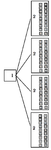
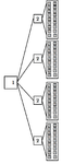
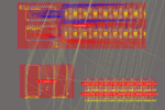
I have a hierarchical design containing a top sheet, which contains four sub sheets, each of which contain 16 sub sheets - 64 in total. I arrange each of the 64 lowest sheets in their individual rooms (fig 1) no problem and arrange them into a grid (fig 2). I then want to connect the components in the middle sheet to that grid and that's where the problem lies - how can I route the components from room to room and then copy this to other groups of rooms? The way I sought to do this was by deleting all individual rooms and drawing a new room around everything, routing the tracks (fig 3) and then copying the room formats - but - it doesn't seem to work as the positions of most of the components aren't arranged properly (fig 4) - though some are!

I am guessing that as this method works with some of the components - the ICs - that I just have to change something and it will work fine when I copy the room formats, but it would be interesting to hear other ways around this problem too..

fig 1
Screenshot 2015-04-08 17.37.58.png
fig 2
Screenshot 2015-04-08 17.38.20.png
fig 3
Screenshot 2015-04-08 17.39.02.png
fig 4
Screenshot 2015-04-08 17.48.31.png
 

In your hierarchical design, you should try to group the lowest subsheets and components in higher subsheets into the groups that will be the same in your pcb layout. So in your fig 4, the large room (2 ics plus the smaller groups) should be one sheet in your hierarchical design. I hope this makes sense :D Altium should be able to create the room for this super group for you and you can copy the room formats.
 

I think I see what you mean - if I rearrange my schematic so I just have a top sheet containing four sub sheets, each of which contain both the ics and the current smallest room. Is that right?

..but, if I have the ICs and the the smaller groups on one sheet, I will have to route them all by hand, which will be a pain. arranging them 1-4-16 clears up the design in the schematic view immensely
 

Attachments

  • roomarrange2.png
    roomarrange2.png
    32.8 KB · Views: 85
  • roomarrange1.png
    roomarrange1.png
    56.9 KB · Views: 100

Ah, you should still use 1-4-16, but is there anything preventing you from creating a subsheet with:

- the 2 ics
- subgroup (which contains the 16 smallest groups)

I think that the structure on the right of the photo you posted. You should be able to eliminate the step where you have to create the new rooms for the larger group on the pcb. Although creatin new rooms should work, you have to make sure the channel offsets are the same, which can be quite a pain too. Try to find a way to build your schematic where altium creates the classes/rooms/offsets for the hierarchical design which allows you mirror rooms on the pcb, as opposed to creating the rooms that need to be copied on the pcb.

The only thing i see that needs to be routed manually is the connections from the smallest groups to the ics. And you should be able to copy this to other rooms afterwards. (Is this the manual routing you mentioned and was against doing?) Can't really offer better suggestions without seeing the whole project though :)
 

hmm, I'm not entirely sure I see what you mean. Here are a few pictures of my project

this is the top sheet view, you can't see everything but this is the part where the 4 middle sheets are defined
layout3.png

the whole of the middle sheet
layout2.png

the whole of the lowest sheet
layout1.png

how would I change the project to include this additional subsheet containing the 2 ICs and the subgroup?
 

Yup, I think that the schematics are ok. Doesn't altium create the rooms for your middle sheet? If it is enabled in your project options, i think it should generate those rooms (along with the rooms for your lowest sheet).

I can't remember where, but you should be able to check if the channel offsets for the components are the same. Unmatched channel offsets could be the reason you couldnt copy the room formats correctly previously. I think when you copy room formats, you could also choose to base it on the designators of the components. Maybe selecting that option will give you a different result?
 
Last edited:

altium does create a room for the middle sheet, but it only contains the ics and two caps, so I'm not sure the best way of getting from that (bottom part of attached fig) to what I want, where the routing is all complete (the top part of attached fig). It seems I can't do this if I leave them as separate rooms.

If I delete all the small rooms, as I have done, and draw a new room around the middle and lower sheets, nothing will match by channel offset. I suppose this is because they all have conflicting channel offsets - all components are named either 1,2,3,4. If I match by source designator, the ICs will match and place but only one of the small rooms is placed properly. I suppose this is because as the ICs have only one version they will match but again, all the designators for the smaller rooms are somehow conflicting.

I suppose there is a way of altering how the designators for the small rooms are generated which might mean that this would work, but I don't fully understand how copy room formats uses the designators to match
 

Attachments

  • newlayout.png
    newlayout.png
    77.2 KB · Views: 141

Status
Not open for further replies.

Part and Inventory Search

Welcome to EDABoard.com

Sponsor

Back
Top