manojkhandelwal
Member level 2
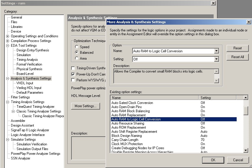
Iam trying to infer MLABs or M512 etc....for my RAM implementation
But even if i apply the ramstyle attribute at the variable declaration ,RAM is not getting inferred.
Does any one know the reason....
But even if i apply the ramstyle attribute at the variable declaration ,RAM is not getting inferred.
Does any one know the reason....