Continue to Site

Welcome to EDAboard.com

Welcome to our site! EDAboard.com is an international Electronics Discussion Forum focused on EDA software, circuits, schematics, books, theory, papers, asic, pld, 8051, DSP, Network, RF, Analog Design, PCB, Service Manuals... and a whole lot more! To participate you need to register. Registration is free. Click here to register now.

Advices and check with high low level pump with Kicad

Status
Not open for further replies.

jmx66

Member level 5
Joined
Nov 16, 2010
Messages
93
Helped
0
Reputation
0
Reaction score
1
Trophy points
1,288
Location
France
Activity points
2,045
Hi all,

I'm not an experienced '' designer '' with Kicad ...., but I really like open source softs and more precisely Kicad, BRL cad, and FreeCad.

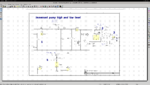
My board is a basic one; only to monitor and switch on - off, an immersed pump for a water pool.

SSR choice: SSR RA4850

If someone would check this crude schematic, would be great before wasting time and money to etch boards.

Thanks guys, and nice day.

Jm Immersed_Pump_Capture_Screen.png
Kicad_Pcb_Screen_Capture.png
 

Attachments

  • MOS4093PHI_PHI.pdf
    78.9 KB · Views: 71
  • NE555.pdf
    1.5 MB · Views: 70
  • RA4850-D12.pdf
    1,013.5 KB · Views: 73
Hi,

What you did is: just connecting the electronic parts.

But a nowadays PCB layout is much more. No wonder KICAD shows a lot of errors.
It does not follow basic rules.

But this does not mean that it does not work. It may work for one day or one month or all the time...it may may cause malfunction when someone with a cellular phone is close..or other HF sources. Hard to say.

My recommendation:
* Either try it as it is,
* or do some PCB design tutorials first and learn the basics of PCB design.

Klaus
 
  • Like
Reactions: jmx66

    jmx66

    Points: 2
    Helpful Answer Positive Rating
Hi,

What you did is: just connecting the electronic parts.

But a nowadays PCB layout is much more. No wonder KICAD shows a lot of errors.
It does not follow basic rules.

But this does not mean that it does not work. It may work for one day or one month or all the time...it may may cause malfunction when someone with a cellular phone is close..or other HF sources. Hard to say.

My recommendation:
* Either try it as it is,
* or do some PCB design tutorials first and learn the basics of PCB design.

Klaus
Hi Klaus,

Thanks a lot for your quick reply.

I made a pcb, some loooooong time ago with transfert and adhesive tapes.... Old school; it worked perfectly for about 20 years.

Only relay with free wheeling diode, capa and resistor to delay, and classic switch with pnp.

For short, if I want to try my '' new '' schematic, would be a wise search to find how to shield this circuit?


Better to use mechanical milling to perform this job and shielding, the entire pcb?


Nice day.

Jm
 
Last edited:

There is an electrical fault - the 'Manual switch OFF', if the intention is to link the pins together with a switch or jumper, will damage U1B by grounding it's output pin.

You should also add at least one decoupling capacitor across the supply and ground connection. Adding one beside each IC would be better.

In Kicad I would suggest you draw a rectangular zone just inside the edge of the board and flood fill it with ground connection. I would think with a little care you could make it single sided to cut costs.

Brian.
 
Which version of KiCAD do you use and which libraries?
Haven't seen in official libraries square pads on resistors/capacitors/...
And, yes, you will kill U1B with "manual" switch.
 

Hi,

For short, if I want to try my '' new '' schematic, would be a wise search to find how to shield this circuit?

Nowadays circuits should expect nearby HF, like from cellular phones, WLan, Bluetooth....thus I always recommend to use one layer as GND plane.
Best: no other traces in this layer no cuts in this layer. This is not perfect but a good and simple rule.
Only if you are experienced enough, know about (HF) current flow on the board, and know about (unwanted) "antennas" on your PCB.... then you could add some traces, add some cuts into the GND plane.

Better to use mechanical milling to perform this job and shielding, the entire pcb?
You mean to fill the space between the traces of a layer with copper.
No.
No, because this is no shielding at all. If I would rate the HF benefit against a solid GND plane, then I assume it is below 5%.
It's more "show" than true benefit.

I've posted many times before to almost identical threads. Please do a forum search.

Klaus
 
  • Like
Reactions: jmx66

    jmx66

    Points: 2
    Helpful Answer Positive Rating
* It's not clear what is the initial state of U1A. Its inputs have no path to any definite voltage. They're only exposed to capacitors. (A condition described as floating inputs.)

(U1B inputs are connected to ground via 10M resistor which satisfies normal guidelines.)

* In some circumstances both led's D4 D5 are lit.
 
There is an electrical fault - the 'Manual switch OFF', if the intention is to link the pins together with a switch or jumper, will damage U1B by grounding it's output pin.

You should also add at least one decoupling capacitor across the supply and ground connection. Adding one beside each IC would be better.

In Kicad I would suggest you draw a rectangular zone just inside the edge of the board and flood fill it with ground connection. I would think with a little care you could make it single sided to cut costs.

Brian.
Thanks for your reply.
Jm
--- Updated ---

* It's not clear what is the initial state of U1A. Its inputs have no path to any definite voltage. They're only exposed to capacitors. (A condition described as floating inputs.)

(U1B inputs are connected to ground via 10M resistor which satisfies normal guidelines.)

* In some circumstances both led's D4 D5 are lit.
Thanks for your reply.
Jm
 

Hi,


Nowadays circuits should expect nearby HF, like from cellular phones, WLan, Bluetooth....thus I always recommend to use one layer as GND plane.
Best: no other traces in this layer no cuts in this layer. This is no
Hi,

What you did is: just connecting the electronic parts.

But a nowadays PCB layout is much more. No wonder KICAD shows a lot of errors.
It does not follow basic rules.

But this does not mean that it does not work. It may work for one day or one month or all the time...it may may cause malfunction when someone with a cellular phone is close..or other HF sources. Hard to say.

My recommendation:
* Either try it as it is,
* or do some PCB design tutorials first and learn the basics of PCB design.

Klaus

t perfect but a good and simple rule.
Only if you are experienced enough, know about (HF) current flow on the board, and know about (unwanted) "antennas" on your PCB.... then you could add some traces, add some cuts into the GND plane.


You mean to fill the space between the traces of a layer with copper.
No.
No, because this is no shielding at all. If I would rate the HF benefit against a solid GND plane, then I assume it is below 5%.
It's more "show" than true benefit.

I've posted many times before to almost identical threads. Please do a forum search.

Klaus
Hi Klaus, and others membres,
Hi,

What you did is: just connecting the electronic parts.

But a nowadays PCB layout is much more. No wonder KICAD shows a lot of errors.
It does not follow basic rules.

But this does not mean that it does not work. It may work for one day or one month or all the time...it may may cause malfunction when someone with a cellular phone is close..or other HF sources. Hard to say.

My recommendation:
* Either try it as it is,
* or do some PCB design tutorials first and learn the basics of PCB design.

Klaus

Thanks a lot for your
Hi,


Nowadays circuits should expect nearby HF, like from cellular phones, WLan, Bluetooth....thus I always recommend to use one layer as GND plane.
Best: no other traces in this layer no cuts in this layer. This is not perfect but a good and simple rule.
Only if you are experienced enough, know about (HF) current flow on the board, and know about (unwanted) "antennas" on your PCB.... then you could add some traces, add some cuts into the GND plane.


You mean to fill the space between the traces of a layer with copper.
No.
No, because this is no shielding at all. If I would rate the HF benefit against a solid GND plane, then I assume it is below 5%.
It's more "show" than true benefit.

I've posted many times before to almost identical threads. Please do a forum search.

Klaus

* It's not clear what is the initial state of U1A. Its inputs have no path to any definite voltage. They're only exposed to capacitors. (A condition described as floating inputs.)

(U1B inputs are connected to ground via 10M resistor which satisfies normal guidelines.)

* In some circumstances both led's D4 D5 are lit.

Hi,


Nowadays circuits should expect nearby HF, like from cellular phones, WLan, Bluetooth....thus I always recommend to use one layer as GND plane.
Best: no other traces in this layer no cuts in this layer. This is not perfect but a good and simple rule.
Only if you are experienced enough, know about (HF) current flow on the board, and know about (unwanted) "antennas" on your PCB.... then you could add some traces, add some cuts into the GND plane.


You mean to fill the space between the traces of a layer with copper.
No.
No, because this is no shielding at all. If I would rate the HF benefit against a solid GND plane, then I assume it is below 5%.
It's more "show" than true benefit.

I've posted many times before to almost identical threads. Please do a forum search.

Klaus

There is an electrical fault - the 'Manual switch OFF', if the intention is to link the pins together with a switch or jumper, will damage U1B by grounding it's output pin.

You should also add at least one decoupling capacitor across the supply and ground connection. Adding one beside each IC would be better.

In Kicad I would suggest you draw a rectangular zone just inside the edge of the board and flood fill it with ground connection. I would think with a little care you could make it single sided to cut costs.

Brian.

advices, really helped me.
Jm
There is an electrical fault - the 'Manual switch OFF', if the intention is to link the pins together with a switch or jumper, will damage U1B by grounding it's output pin.

You should also add at least one decoupling capacitor across the supply and ground connection. Adding one beside each IC would be better.

In Kicad I would suggest you draw a rectangular zone just inside the edge of the board and flood fill it with ground connection. I would think with a little care you could make it single sided to cut costs.

Brian.
--- Updated ---

Hi Klaus, and others members,

Thanks a lot for your advices, they really helped me.
Jm
 

Hi Klaus, and others membres,


Thanks a lot for your replies.


Your advices, really helped me.
Jm

--- Updated ---
--- Updated ---

Hi all,

I made some changes to the initial schematic, after reading your previous replies.

1 Resistor 10 MOhm for U1A input

2 Polarised capacitor 63 v 680 µF CP
Ceramic capacitor 100 nF C7

3 Manual switch for stop

4 Ceramic C8 C3XX-X7R

To do:

Read, and read and read, about Ground Plane + tin box shielding ....

Led D4 and D5 to check ( See jpg)


Any mistakes?

Thanks a lot.

Jm
 

Attachments

  • Immersed-Pump-High-Low-Level.png
    Immersed-Pump-High-Low-Level.png
    112.7 KB · Views: 95
  • waveforms-tim44.gif
    waveforms-tim44.gif
    11.6 KB · Views: 91
Last edited:

Status
Not open for further replies.

Part and Inventory Search

Welcome to EDABoard.com

Sponsor

Back
Top