mohamis288
Full Member level 3
Hi,
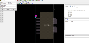
I had designed a footprint for a special component named AFIC10275N and I want to replace my designed footprint with footprint of this IC which is available in the library. BUT, this IC is read-only and it seems that I can not change its layout. the most important point is that the layout of this IC is very large( maybe in the layout the size of the layout is 40 times bigger than the whole size of the board.) also ,there are some connection in the schematic but when I update the layout, there are no relative connection in the layout. definitely, I need IC layout to perform EM analysis. moreover, I think it is overwhelming to design the test circuit in the schematic and then transfer them to the layout ( it is better to design the circuit in the layout and then transfer the layout to schematic.). anyway, I need a good layout. if can not provide a good layout, I have to do simulation in the schematic only?
I think I am not allowed to share the full datasheet in the attachment. you can download it by searching AFIC10275N. the related document are available in NXP website. anyway, I attach some picture about my problem.
Attachments
Last edited: