Continue to Site

Welcome to EDAboard.com

Welcome to our site! EDAboard.com is an international Electronics Discussion Forum focused on EDA software, circuits, schematics, books, theory, papers, asic, pld, 8051, DSP, Network, RF, Analog Design, PCB, Service Manuals... and a whole lot more! To participate you need to register. Registration is free. Click here to register now.

adc0804 interfacing with fpga

Status
Not open for further replies.

Maxima8

Newbie
Joined
Apr 21, 2015
Messages
3
Helped
0
Reputation
0
Reaction score
0
Trophy points
1,281
Activity points
1,305
Hi guys.

I am beginner in fpga. So i need help for my project. I have used 16 adc0804 in my project. The input for adc is from my 16 receiver curcuit. And now I want to interface the adc with FPGA. But i am very confusing. From my understanding, the output from adc0804 is digital. So, i just need to connect the output at DBn to gpio of de2 board. Is it correct guys? kindly help me please:-:)-:)-(
 

Hi shaiko.

Thanks for your reply. Yes. it is my adc that i have used. So, do you mean that i just connect the DBn, intr, cs,wr, rd to GPIO of FPGA? Then i need to control cs,wr,rd signal? Could you explain little bit more detail. I still confuse.
 

DBn, intr, cs,wr, rd to GPIO of FPGA
Yes,
Together with the data pins. That's quite a bit of wires...

Afterwards, you'll have to implement the control logic according to the waveforms in page 7.
 

The solution is not completely obvious, there are different options:

- Implementing a common data bus for all ADCs, sequentially accessing the data
Advantage: less FPGA pins
Disadvantage: more complex logic

- Individual data lines for each ADC
Advantage: Simple logic, fast access without sequences. Some ADC pins can be connected to fixed level, at least nCS.
Disadvantage: many FPGA pins needed
 

First you need to think on how you can reduce the number of ADCs from 16 to some convenient number say 4 or 5. Then it will be easier for you to think of interfacing ADCs to the fpga.

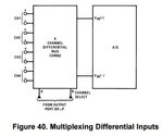
if you use a 'n' channel diff mux, things will be much simpler. Refer to the attached figure taken from the DS. This should help you. Later try using a configuration similar to Fig 61 - Interfacing Multiple A/Ds in an MC6800 System.
 

Attachments

  • ADC.JPG
    ADC.JPG
    22.3 KB · Views: 84

Yes,
Together with the data pins. That's quite a bit of wires...

Afterwards, you'll have to implement the control logic according to the waveforms in page 7.


Hi shaiko.

Thanks for your reply. I am very very beginner in vhdl. I have write some code for the adc and i know its wrong. But could you give me some ideas how to build the vhdl :cry::cry:
 

Attachments

  • new 1.txt
    661 bytes · Views: 81

1. Your code won't compile due to syntax issues.
2. Even if it would compile - it won't synthesize. You can't use "after" to describe real logic.

I suggest you acquire minimal VHDL skills before you continue
Please watch this video:

**broken link removed**
 

Status
Not open for further replies.

Similar threads

Part and Inventory Search

Welcome to EDABoard.com

Sponsor

Back
Top