Continue to Site

Welcome to EDAboard.com

Welcome to our site! EDAboard.com is an international Electronics Discussion Forum focused on EDA software, circuits, schematics, books, theory, papers, asic, pld, 8051, DSP, Network, RF, Analog Design, PCB, Service Manuals... and a whole lot more! To participate you need to register. Registration is free. Click here to register now.

[SOLVED] Adc0804 interfacing doubts

Status
Not open for further replies.

thannara123

Advanced Member level 5
Joined
Jan 7, 2010
Messages
1,580
Helped
122
Reputation
244
Reaction score
114
Trophy points
1,353
Location
India
Activity points
10,381
hello ,experts
i read the datasheet of adc0804 .and wrote a program to convert the analog input (through adc0804)
program follwos
sbit rd = P3 ^ 3; // declare P3.3 as rw pin
sbit cs = P3 ^ 4; // declare p3.4 as cs pin
sbit wr = P3 ^ 5; // declare p3.5 as read/write pin
sbit intr = P3 ^ 6;
unsigned char gk;
void conv(); //Start of conversion function
void read(); //Read ADC function


void conv()
{
cs = 0; //Make CS low
wr = 0; //Make WR low
wr = 1; //Make WR high
//cs = 1; //Make CS high
while (intr); //Wait for INTR to go low
}

void read()
{

cs = 0; //Make CS low
rd = 0; //Make RD low
gk = P1; //Read ADC port
rd = 1; //Make RD high
// cs = 1;
//Make CS high
[FONT='Courier New', Courier, monospace]}[/FONT]
[FONT='Courier New', Courier, monospace]i need the pin intr,rd,cs,wr [/FONT]
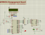
[FONT='Courier New', Courier, monospace]But in development Board has some pins are shorted , something like see the picture
[/FONT]
eda.JPG

why the pin INTR and WR are shorted,
CS and RD pin are shorted >and given to ground (if so how can i read the data without giving High to RD pin)
please help me thanks
 

Pin Description
1. CS, Chip Select:
2. RD, Read: This is an input pin and active low. After converting the analog data, the ADC stores the result in an internal register. This pin is used to get the data out of the ADC 0804 chip. When CS=0 & high to low pulse is given to this pin, the digital output is shown on the pins D0-D7.
3. WR, Write: This is an input pin and active low. This is used to instruct the ADC to start the conversion process. If CS=0 and WR makes a low to high transition, the ADC starts the conversion process.
4. CLK IN, Clock IN: This is an input pin connected to an external clock source.
5. INTR, Interrupt: This is an active low output pin. This pin goes low when the conversion is over.
6. Vin+ : Analog Input .
7. Vin- : Analog Input. Connected to ground.
8. AGND: Analog Ground.
9. Vref/2: This pin is used to set the reference voltage. If this is not connected the default reference voltage is 5V. In some application it is required to reduce the step size. This can be done by using this pin.
10. DGND: Digital Ground.
11-18. Output Data Bits (D7-D0).
19. CLKR: Clock Reset.
20. Vcc: Positive Supply

Pls Read This and
and follow the below link...
ADC Interfacing - MATLAB ACADEMY

Here is a small tutorial on ADC0804 Interfacing with AT89C51 Micro-Controller along with Program...
 

Adc_Schematic.PNG

Use This Schematic...
It is Correct and tested by me...

And for More Information Read Datasheet and the Timing Clocks of each pins..

Hope this helps you...
 

As Arun Sharma said WR is used to instruct the ADC to start the conversion process. Maybe after power on WR can be H or L (this condition is not predictable). Unfortunately, when power on INT is High, to start conversion, you have to push that switch, WR becomes L and conversion is started. The conversion will start and start again because when conversion is finished, INT pin becomes Low and it is received by WR (Free running). It's better you send Low shortly to WR-INT junction from software at top line of your program, so you don't need to push switch to start conversion. To avoid logical conflict between INT and your microcontroller's pin, you can add a diode, anode to the junction and cathode to microcontroller's pin. Pulse it Low shortly and then back to High.
 

thanks But am asking regarding my development board (see the image in first post ) there the PINs 1 an 2 (Cs & RD)are shorted
also PINs 3 and 5 (WR & INTR )are shorted
why so , then how i can sen individually signals to each pins
 

actually pin 1 and pin 2 are not aimed shorted, but these pins are connected to ground. these pins are not affected each other but they are affected by ground. and at the picture, that's just to make drawing easier. Pin 1 is connected to ground to make the chip works. Pin 2 is connected to ground to make the output can be read by the others.

pin 3 and pin 5 are shorted to make free running conversion.
the conversion of ADC can not be start if we don't push the switch, because conversion only will be started if pin 3 is Low. After the conversion is started, pin 5 will be high and then pin 5 will be Low when the conversion is finished.
To start new conversion, we have to give Low condition to pin 3, and it's meant we have to push the switch again or ........ we can use pin 5.
Now, the conversion will be started again, although we don't push the switch, because the pushing of the switch has been took over and handled by pulse condition of pin 5.
 
solved .i disconnected the wire that is where the INTR and the WR shorted .
 

Status
Not open for further replies.

Similar threads

Part and Inventory Search

Welcome to EDABoard.com

Sponsor

Back
Top