Continue to Site

Welcome to EDAboard.com

Welcome to our site! EDAboard.com is an international Electronics Discussion Forum focused on EDA software, circuits, schematics, books, theory, papers, asic, pld, 8051, DSP, Network, RF, Analog Design, PCB, Service Manuals... and a whole lot more! To participate you need to register. Registration is free. Click here to register now.

[SOLVED] ADC DNL/INL measurement prior to calibration

Status
Not open for further replies.

dirac16

Member level 5
Joined
Jan 20, 2021
Messages
87
Helped
0
Reputation
0
Reaction score
0
Trophy points
6
Activity points
677
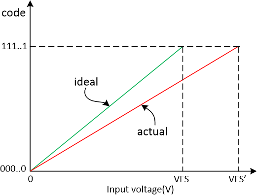
In the following image the actual transfer function falls off because of the negative gain error. What usually is done in software is to compensate for the gain error using best fit line method or other ones as per the designer and the application requirements.
figures.png


I am working on an ADC where the specs need to be reported before calibration is performed. Unfortunately, the ADC's actual transfer function has significant negative gain error (as shown above) and for that reason I want to measure DNL/INL before doing any a priori calibration (That is to showcase the importance of the post calibration on the measured data). The problem is that I am not sure enough as to how DNL and INL are measured in the presence of the gain error. Particularly, how is the LSB size found in the above figure? Should I only extend the VFS to the actual VFS' and rewrite the LSB size based on VFS'? Then the calculation of the DNL/INL based on the newly updated LSB will be straightforward. Please tell me if I am right.
 

Solution
Well, we get FS error with positive gain error too, but nevermind.
When real measured characteristic have smaller gain than the ideal slope, in your terminology when it has negative gain error, that means a measured code represents a higher voltage than the actual signal has. That is all.

And If you know the exact error values, obviously you can do a correction, and it is recommended, since the ideal characteristic is the target which can represent the actual signal.

Real measured data errors usually cannot be compensated, or extra effort, this is why designers want to keep these low, like DNL or INL. But in digital, or even in analog domain sometimes it is not so big effort to add/subtract an offset, or multiply/divide the data...
I think you are right, rewrite LSB size is the way how the gain error is removed from the characteristic.
DNL/INL in LSB' unit should be the same as DNL/INL in LSB.
 

Hi,

DNL and INL ar nonlinearities and usually refer to "LSB" as unit.
So they don´t refer to an absolute voltage error .. with unit "V".
(This may be different with your requirement - please tell us.)

Then DNL as well as INL usually are independet of the gain and it´s error.

Your graph shows
* perfect offset - which is not expectable
* perfect INL and DNL - which is not expectable
* pure gain error

*****
Now you ask about the value of LSB without giving any usful inoformation.
The ADC designer (or the datasheet) should know
* the nominal analog ADC output voltage range (example: 0...VRef, or 0...5.0V, or -2.5V ... +2.5V)
* the adc resolution in bits (example: 10 bits, 16 bits)

Then the nominal ADC LSB value is: V_LSB = ADC_range / 2^ADC_bits
Example: on a 10 bit ADC with a 0...5.0V output voltage range: V_LSB = 5V / 2^10 = 5V / 1024 = 4.883mV

****
Real ADCs have
* offset errors
* gain errors
* DNL and INL errors
* may have "rail" problems. In this case you should exclude measurements at output voltages close to the rail.

Example:
* 10 bit ADC, Range 0V...5V, perfect gain
* -20mV offset error
* +50mV saturation voltage to GND
1634467943418.png


Klaus
 

Hi,

DNL and INL ar nonlinearities and usually refer to "LSB" as unit.
So they don´t refer to an absolute voltage error .. with unit "V".
(This may be different with your requirement - please tell us.)

Then DNL as well as INL usually are independet of the gain and it´s error.

Your graph shows
* perfect offset - which is not expectable
* perfect INL and DNL - which is not expectable
* pure gain error

*****
Now you ask about the value of LSB without giving any usful inoformation.
The ADC designer (or the datasheet) should know
* the nominal analog ADC output voltage range (example: 0...VRef, or 0...5.0V, or -2.5V ... +2.5V)
* the adc resolution in bits (example: 10 bits, 16 bits)

Then the nominal ADC LSB value is: V_LSB = ADC_range / 2^ADC_bits
Example: on a 10 bit ADC with a 0...5.0V output voltage range: V_LSB = 5V / 2^10 = 5V / 1024 = 4.883mV

****
Real ADCs have
* offset errors
* gain errors
* DNL and INL errors
* may have "rail" problems. In this case you should exclude measurements at output voltages close to the rail.

Example:
* 10 bit ADC, Range 0V...5V, perfect gain
* -20mV offset error
* +50mV saturation voltage to GND
View attachment 172427

Klaus
Thanks for the answer. Yes, the actual gain error I am watching is not that perfect and has some wiggles in it. The thing yet I am not sure about is I do not understand why one would go for gain correction if DNL/INL measurements are independent of the gain error? What is gain correction useful for? The second thing yet I do not get is the actual LSB size in the presence of the gain error. How do you determine that? If it is still VFS/2^N then we would get full scale error where some of the output codes would be unused for negative gain error. And similarly, if the gain error is positive some of the input range would be lost. Should I then report on my DNL/INL measurements even though I do have full scale error?
 
Last edited:

DNL/INL measurements are not independent of gain error. You have to calculate the correct LSB size to make it independent, and you have to do it with removing the gain and offset errors.

You determine the LSB size with curve fitting. It can be startpoint/endpoint fit, LMS approximation method, whatever, and the fitted curve's steepness or derivate is the LSB itself.
Thank you, it makes pretty much sense now. There is a thing yet however. As you know for negative gain error we get full scale error. So, for example, after the startpoint/endpoint fit method is done on the actual curve, should we then divide the ideal slope by the fitted curve's slope and multiply the ratio by the measured data to remove FS error?
 

Well, we get FS error with positive gain error too, but nevermind.
When real measured characteristic have smaller gain than the ideal slope, in your terminology when it has negative gain error, that means a measured code represents a higher voltage than the actual signal has. That is all.

And If you know the exact error values, obviously you can do a correction, and it is recommended, since the ideal characteristic is the target which can represent the actual signal.

Real measured data errors usually cannot be compensated, or extra effort, this is why designers want to keep these low, like DNL or INL. But in digital, or even in analog domain sometimes it is not so big effort to add/subtract an offset, or multiply/divide the data with a gain factor, apply auto-zeroing,/choppering circuits.
 
Solution
Noticed that to some extend gain error could be repesented by INL, indeed the definition of INL has already implyed it is non-learity which would has affection on learity(gain error). The DNL/INL would be like below accroding your image.
capture-2021-10-19-09-33-57.png

So you should remove your gain error first to get the DNL/INL purely affected by matching, parasitics or other non-ideal factors. Then your post calibration could help more obviously with reasonable DNL/INL(smaller and independent from gain error).
 

Hi,

I think there is some confusion.

I still think the DNL/INL given in an ADC datasheet is independent of it´s gain error.

And I agree that the DNL/INL measurement has to include real LSB size to get the DNL/INL value to be independent.

But there is no need to calibrate the ADC. It´s sufficient to measure and calculate the real LSB size.
Due to unlinearities and other problems this sometimes is done at let´s say 10% level and 90% level

like: V_LSB = (V_90% - V_10%) / (2^n * 80%)

And in such a case the offset is not involved at all.

For sure one may also find it using best_fit_linear method. Also here i´d use 10% to 90% (or similar) only.
I wonder if it makes a meaningful difference on a real ADC.

****
Different ADCs have different DNL/INL behaviour. Some SAR ADCs suffer from high DNL at 1/2, 1/4 and 3/4 of code, when multiple bits switch (code from 0b01 1111 111 to 0b10 000 000). Some even suffer from missing codes here.

On an ADS8320 I experienced missing codes (within datsheet specifications = 14 bit), but could improve it with adding a bigger (than datasheet recommendation) capacitance to the VRef pin. Then I had no missing codes up to 16 bit.

Klaus
 

In addition, not in every datasheet there is the same formula. Someone likes when all errors combined, which distorts the non-linearity measurement, but shows which error is more significant. Who cares missing codes if gain error is huge and vice versa.
 

Status
Not open for further replies.

Similar threads

Part and Inventory Search

Welcome to EDABoard.com

Sponsor

Back
Top