Continue to Site

Welcome to EDAboard.com

Welcome to our site! EDAboard.com is an international Electronics Discussion Forum focused on EDA software, circuits, schematics, books, theory, papers, asic, pld, 8051, DSP, Network, RF, Analog Design, PCB, Service Manuals... and a whole lot more! To participate you need to register. Registration is free. Click here to register now.

adc and dac in a circuit grounding tips?

Status
Not open for further replies.

seyyah

Advanced Member level 2
Joined
Oct 7, 2001
Messages
646
Helped
8
Reputation
16
Reaction score
8
Trophy points
1,298
Activity points
6,233
I have an ADC in my system and a DAC. How should i design the ground plane, any tips? The board will be 4 layered. I have a 3.3V mcu.
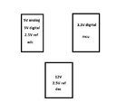
ADC and DAC has a 2.5 reference in common. DAC requires a 12V voltage source. Digital section of the ADC can operate at 3.3V or 5V but i plan to use 5V. Analog voltage supply of the ADC is 5V.
I would appreciate any suggestion on planning the powers and grounds of the pcb, thanks
 

Attachments

  • pcb.jpg
    pcb.jpg
    22.2 KB · Views: 116

use only one ground plane, but partition it into analog and digital. they are joined together under the ADC. Don't cross any signal over the split. they only cross over the bridge between analog and digital ground.
a/d and d/a are considered analog components. these are analog ic that have a digital section.

AD_GND.jpg
 
  • Like
Reactions: seyyah

    seyyah

    Points: 2
    Helpful Answer Positive Rating
I am an engineer designed a lot of data acquisition systems. I worked for LeCroy that manufacture transient recorders and now digital scopes. I use ONE solid ground plane. I don't separate ground.

Signal travel as EM wave, not current and voltage like most people think. The traces on pcb is regarded as microstrip or stripline in higher speed signals like the digital signals. The ground return current stay right under the signal trace. The last thing you want is the have split ground and have signal traces cross from one ground plane to the other. That's when you create a lot of emission and radiate to other sensitive circuits. If you split ground plane, you have to really know how to route the trace so it does not see a break in the return image current. One violation and you might have problem.

The best way to deal with mixed analog and digital circuit that have low current signal ( this apply to your case) is to pay attention how you route the digital traces so they don't run on or across the analog section. The very important thing to know is the return current of the signal trace concentrates on the ground plane right under the trace, I forgot the formula of the dielectric thickness relation, 90 to 95% of the return current are contain within 5 trace width of the ground plane on each side under the signal trace on a normal 4 layer board. So if you have analog like 10 signal trace width from the digital signal trace, you are not going to have a lot of problem......IF you don't have signal that jump from one to the other ground plane that cause a break of the return image current.

This goes for power plane. For 4 layers, chances are you have split power planes. Say you have the split power plane on the layer above the bottom layer and you have traces on the bottom. You can have problem crossing from one power plane to the other. Power plane on the 4 layer board should be very close to the ground plane. Usually I put only 5 mil spacing between ground and power plane so I create a sheet of capacitance to couple the power to ground plane. Then I put 0.01 capacitors at regular interval along the edge of the ground plane along the split power plane so this create a current path for the return image current of the signals.

This is a big topics, I am just cover the very basic stuff on Signal Integrity engineering. I practice all these when I was working as a Signal Integrity engineer for a little while. PCB designing is so much more than just learning a layout package and placing components. I encourage pcb designers to take a class or at least a seminar on signal integrity.

Only time I ever use split ground is in MOSFET circuits where it takes a lot of power to drive the capacitance of the gate and that actually make the whole ground plane jump. But for low power circuits, don't cut ground.

On the side note, when you create fan out for BGAs, watch out the thermal relieves and ground connections under the BGA. I worked on a board that the pcb designer did not pay attention, you look at the ground plane under the BGA, the ground plane got cut up into pieces and totally lost the plane. Then the pc designer was stupid enough to just route the ground with traces blindly when design rule check point the error out!!! Don't rely too much on the layout package to do the signal integrity for you, you have to pay attention on things or it can really go wrong. All the pcb layout software are nothing more than like MS Word, it's a tool, nothing more. It is still you behind the pcb.
 
Last edited:
  • Like
Reactions: seyyah

    seyyah

    Points: 2
    Helpful Answer Positive Rating
Thanks for the replies and tips. I may design the board in two pieces and connect them with a connector because the board area is small. One board can contain analog supply and parts and the other board can contain digital supply and mcu and other things. Problem is, adc and dac should communicate with mcu over spi signals which may be at the rates of hundreds KHz to 10MHz. The spi signal will be at 5V level and will be generated at analog board. So it should be taken to the digital board. So how should i route these signals and power and how should i connect two ground planes? Thanks.
 

Now I have a little better idea about your circuit. Your analog circuit is not high speed as you only use SPI bus. I don't think you need to split into two boards. You still have digital on the analog as you have the SPI interface.

But if that's what you want, read my original post again. It is the proximity that is very important. Digital return current on the ground plane stay closely under the trace, so make sure you have all the digital signals stay clear of the analog circuit. Have the analog input and circuit on one side of the board, all the digital circuit on the other side, the SPI come out on the side of the digital circuit.

I take that you plug the small analog board onto the digital board by a connector. Make sure you have plenty of ground pins, each pin accompanies one signal of the SPI. You don't need to add any more ground connection after that. So you have input analog signal and ground, going through the analog board, then ground connects through the SPI connector to the digital board.

Again, you don't need to split board. I pack dense surface mount mixed signal circuits together all the time. I worked with very low level signals of uV range. On very sensitive circuit, I use 6 layer boards, I have two ground layers and put the split power plane sandwiched between the two ground layers so I don't have to worry about the split power plane. The two ground planes are continuous, no splitting. My last design was a mixed signal board with 16 channel 400MHz bandwidth each with gain of about 50 to 100. Converting into pulses by comparators and feed into FIFO so slow down the read out speed. All in a 12"X10" board.


Lastly and most important.............Are you an engineer or pcb designer? If you are pcb designer, let the engineer make the decision. It's really not your problem, let the engineer decide and it'll be his responsibility. I am talking to you as an engineer and I make my decision and I am responsible 100% for my board. As a pcb designer, you are not responsible for this. I am not a pcb designer, I just layout my own boards as it is not efficient to work with a pcb designer in very critical mixed signal boards. AND ultimately, I am 100% responsible for the board.
 
Last edited:

Ok i understand mostly. I am the engineer, I was not designing pcbs for a while but since this is a bit sensitive i want to design this board myself. The board area is approximately 5"x6". I plan to create 2 same size boards. Analog is at the bottom and digital is on the top. Actually i don't need to split the board currently but after i verify this board i plan to expand functionalities of the digital part in the future so 2 boards give me tjhe flexibility i think.
 

If one board is stacked on top of the other, the ground pins in the connector from the analog board to the digital board is good enough already. As I said, make sure you have one ground pin next to one signal in the connector. Make sure each of the ground pin tie directly onto the ground plane.

This is a good introduction level of signal integrity, it's good to keep a copy:

https://www.amazon.com/High-Speed-Digital-Design-Handbook/dp/0133957241/ref=sr_1_1?ie=UTF8&qid=1354427327&sr=8-1&keywords=black+magic+howard+johnson

Since you are an engineer, I can talk in terms of electronic theory, you should understand that signal travel as EM wave with the trace and the ground plane forming a guided structure. Like DC current travel in the path of least resistance, EM wave travel in the path of least impedance.....which is right under the trace. You can make the trace snake around and the current will follow. The signal forward and return path form a loop with cross sectional area. Total flux is the B times the cross sectional area. The bigger the area of the loop, the more flux generated by the same current passing through. To minimize emission, you minimize the loop area. Remember the image current path I was talking about? Any break in the current path will cause the return current to find an alternate path and increase the area of the loop, so the total flux increase. The same goes for the input signal path. Any break in return current will force the return current to find a new path and increase the loop area. Input with a bigger loop is much more sensitive to the stray magnetic flux. This is the theory behind my very first post. This is all electromagnetics.

As most current concentrate under the trace, if you have other signal farther apart, you won't have problem as long as no breakage of the return path. that's the reason it is not important to cut ground plane. Only time is necessary is if current drawn is high and can bounce the whole plane.

That's the reason I layout my own boards, I don't want to keep spending time to explain and people don't trust you!!!!
 
Last edited:
  • Like
Reactions: seyyah

    seyyah

    Points: 2
    Helpful Answer Positive Rating
Thank you very much for your tips you've been most helpful. What do you think about power supply issue. I mean is it better to place voltage regulator near the adc and dac or should it be a bit seperate?
 

Thank you very much for your tips you've been most helpful. What do you think about power supply issue. I mean is it better to place voltage regulator near the adc and dac or should it be a bit seperate?

If it is linear regulator, it doesn't matter. If it is switching or DC/DC regulator, stay away from the analog if possible. Again, breaking of returning image current is more important. I put DC/DC converters quite close to analog circuits also.......I have no choice.
 

Status
Not open for further replies.

Part and Inventory Search

Welcome to EDABoard.com

Sponsor

Back
Top