Continue to Site

Welcome to EDAboard.com

Welcome to our site! EDAboard.com is an international Electronics Discussion Forum focused on EDA software, circuits, schematics, books, theory, papers, asic, pld, 8051, DSP, Network, RF, Analog Design, PCB, Service Manuals... and a whole lot more! To participate you need to register. Registration is free. Click here to register now.

AD9643 SPI Write Problem

Status
Not open for further replies.

jason_bill

Junior Member level 2
Joined
Sep 25, 2013
Messages
20
Helped
0
Reputation
0
Reaction score
0
Trophy points
1
Activity points
152
Hi,

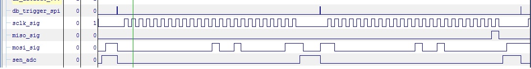
I want to write to the AD9643 Register through SPI interface by FPGA.
I have developed spi core. Read operation work correctly becuase when i read value of register
it returns the default values as same as is mentioned in the data sheet.

But the write operation not work. for example i want to set the 0x0B to 0X03 such as picture 1 but it returns default value again!
7194214700_1428240994.jpg
 

SPI clock phase doesn't seem to be right in the diagram, also the meaning of MISO and MOSi signals isn't clear because AD9643 has a bidirectional SDIO line.
 

Thanks,
I assigned SDIO as below:
Code:
assign sdio = (spi_dir)? 1'bz : mosi_sig; 
assign miso_sig = (spi_dir)? sdio : 1'b0;
when R/W bit equal '1' spi_dir is asserted by spi core.
 

when R/W bit equal '1' spi_dir is asserted by spi core
I presume, it's asserted in the data phase only.

More generally speaking, you have a Verilog design operating the interface, of course the timing diagram doesn't give the design details. Did you understand about the wrong clock phase that I mentioned?
 

Status
Not open for further replies.

Part and Inventory Search

Welcome to EDABoard.com

Sponsor

Back
Top