Continue to Site

Welcome to EDAboard.com

Welcome to our site! EDAboard.com is an international Electronics Discussion Forum focused on EDA software, circuits, schematics, books, theory, papers, asic, pld, 8051, DSP, Network, RF, Analog Design, PCB, Service Manuals... and a whole lot more! To participate you need to register. Registration is free. Click here to register now.

Ad8099 cascade .

Status
Not open for further replies.

Paul98

Member level 5
Joined
Sep 7, 2020
Messages
86
Helped
1
Reputation
2
Reaction score
0
Trophy points
6
Activity points
647
Hello everyone, I found this pattern from another discussion group with 4 cascaded OpAmp. What do you think? It is valid? . Basically it is a scheme also contained in the datasheet and here it is repeated 4 times in series.

Datasheet


Thank you.

AAA 537 16.31.gif
 

I do not see this cascade in the datasheet for starters. Basiclaly this produces a G ~= 1000.

There will be a BW reduction from that of a single stage due to pole shrinkage factor.

1602621023187.png


What is your actual goal (specs) and application ?

Regards, Dana.
 

Hi,

It's like chaining 4 cars. You may do it.
The question is: what do you want to achieve? What's the input signal, whats the load?

Klaus
 

The calculatory gain is about 11000. You need better power supply decoupling and RF shielding to avoid self oscillation. Amplifier noise will be several 100 mVrms at the output.
 

I would like to create a circuit that allows you to amplify very low signals for example 10 / 100uV and to be able to couple it to an MMIC for example. All this with a bandwidth ranging from DC to 500Mhz or even 1Ghz if possible. This OpAmp was suggested to me (thanks) because it allows you to amplify very low signals of the order of 100uV or maybe even less with a bandwidth of about 500Mhz (if there was a component that also reached a 1Ghz bandwith I would not reject it but I it seems to have understood that there are many limitations in this sense. My idea is to create a first stage that allows you to amplify these very low signals and bring it to such a voltage that it can be managed by a subsequent stage like an MMIC. addocciati some but now I would like to better define these first stages. I used 4 stages precisely because on the official datasheet there is no mention of Gain over 20 if I remember correctly and actually I also had the doubt if it could be done or not. I used the one with Gain 10 (the one with G = 20 changes a resistance) in order to have a x10 on each stage so for 100uV input signals:

1) 100uV = 1mV
2) 1mV = 10mV
3) 10mV = 100mV
4) 100mV = 1Volt

if I had 10uV in input it would be:

1) 10uV = 100uV
2) 100uV = 1mV
3) 1mV = 10mV
4) 10mV = 100mV

Besides, I would need to have all the possible bandwidth from DC up to 500Mhz. Actually between the third and fourth stage I could

This simulation scheme does not give any particular problems and works. The problem is that in simulation I don't have the possibility to go up much with the input frequency and actually I don't know the behavior beyond 100Mhz. As for the power supply I have already designed it and it is supplied by an LM337 and an LM338 but I have not foreseen any filter inductance (it is a good advice in fact) I have to put one on each single stage or one for all four the stages on the outputs of the regulators?). Initially I had used fixed regulators of the 78xx and 79xx series but in simulation I had problems (and I don't understand why). Thanks everyone for your help and sorry for the mistakes !. I hope I have answered everyone!
 

Why doesn't anyone answer every time I explain what I want to do @FvM @KlausST ?
 

Hi,

The problem is that in simulation I don't have the possibility to go up much with the input frequency and actually I don't know the behavior beyond 100Mhz.

which simulation tool are you using? I have performed simulations including the appropriate AD8099 spice model provided by AD in LTspice up to several GHz. Where does your simulation-frequency limitation come from?

BR
 

Hi,
Why doesn't anyone answer every time I explain what I want to do @FvM @KlausST ?
My answer is: I can't give a suitable answer, because I dont have enough experience in this range of frequency.

Klaus
 
Last edited:
Before continuing I would like to make a necessary clarification. I think I was misunderstood when I asked why no one answered me. I asked this question because in the first post I immediately received an answer (and that's okay!) But then nobody answered and I asked myself "did I say or do something wrong?" and I asked for explanations publicly because I didn't see anything wrong with it. I mentioned the moderators because they are the moderators and not because I wanted technical answers. Then I was pointed out (even privately) that it is not always possible to have the answers and it is better to refrain (and rightly so). I thought it was a simple question but it probably wasn't. Be patient. Thank you.

About @stenzer question. I am currently using proteus which provides real-time simulation. I am that it is not a permanent solution for many reasons. I could use LTSpice too but I should learn how to use it. There would also be Kikad that should offer the simulation. I have used Kikad for a long time, then I often have it because it did not simulate and I think I understand that it is not officially supported. The problem with Proteus is that it has a large but not very large Spice library. I often look for components that don't have simulation available. I'm looking at LTSpice, is the library for AD8099 already included or did you add it yourself?
 
Last edited:

    KlausST

    Points: 2
    Helpful Answer Positive Rating
Hi,

I included it by my own, but it is a pretty straight forward process. Have a look at [1] (~9:1 min). If there are any problems feel free to ask, and we will help you as good as possible.

[1]

BR
 

Attachments

  • 2.JPG
    2.JPG
    31.5 KB · Views: 180
  • 3.JPG
    3.JPG
    83.5 KB · Views: 192

Hi,

first please connect the electrolytic capacitor C2 in the right way, you have flipped it by means of connecting + to the more negative potentioal.

Please also connect the output of the opamp to a resisive load e.g. 100 k.

Further, you are performing a DC operating point analysis (.op). I assume you are interested in a transient [1] or an AC [2] analysis.

Please let us know in which kind of analysis you are interested in.

[1] https://spiceman.net/ltspice-transient-analysis/
[2] https://spiceman.net/ltspice-ac-analysis/

BR
 

    Paul98

    Points: 2
    Helpful Answer Positive Rating
Hi,

see attached the AC spice simulation result obtained by the use of LTspice.

EDAboard_AD8099.png


I noticed your model does not provide the Disable/Power Down (PD) pin. Have a look in the spice file, there you can see the pin assignement as following. The PD pin is highlighted below.

EDAboard_AD8099_SpiceFile.png


This pin does not cause any troubles as the AD8099 is enabled if this pin is left floating. I assume it is your NC pin. Nevertheless, get used to import the models appropriate as assigned in the spice file, so you can work with them also after a couple of months or years (everthing is clear defined).

BR
 

    Paul98

    Points: 2
    Helpful Answer Positive Rating
I have not foreseen any filter inductance (it is a good advice in fact) I have to put one on each single stage or one for all four the stages on the outputs of the regulators?).
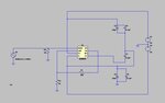
A single filter stage is probably insufficient for a high gain RF amplifier. A popular scheme is a filter chain with increasing attenuation for the most sensitive stage. Suggest to start with lower gain, e.g. 2 stages.
 

    Paul98

    Points: 2
    Helpful Answer Positive Rating
What concerns me is the slew rate with the two following requirements:

4) 100mV = 1Volt

a bandwidth of about 500Mhz

If the last stage has to provide an amplitude of 1 V at a frequency of 500 MHz the required slew rate for a sinewave is determined by

SR = 2 \[\cdot\] \[\pi\] \[\cdot\] f \[\cdot\] \[\hat{V}\] = 2 \[\cdot\] \[\pi\] \[\cdot\] 500 \[\cdot\] \[{10}^{6}\] Hz \[\cdot\] 1 V = 3141.6 \[\frac{V}{µs}\]. According to the datasheet the AD8099 provides only 1350 \[\frac{V}{µs}\] at an amplification of 10.

But as already pointed out in post #2, a bandwidth reduction will occure and the maximum "un-attenuated" frequency is lower.

BR
 

A handy method to multiply gain of transistors is to cascade them by alternating N-type with P-type. The arrangement is like overlapping sziklai pairs. In effect each stage provides bias to the next stage.

This method has reduced parts count as compared to using all N-type, say.
 

Forgive the mistakes, (especially the no load output) correcting them I got the same result as @stenzer so I would say the circuit is ok. I can confirm that I changed the pin names in NC to make them more understandable. Because when I placed the OpAmp the pins had these numbers (101,102,103 ....) which were more distracting. And thanks also for calculating the slew rate. I also welcome @FvM's advice which is what I had thought about creating multiple states in series. In fact on the other software I had put 4 in series but all with G = 10. I try to do the first state with a limited Gain and then let's see how the circuit progresses. For @BradtheRad's post about sziklai pairs configuration it seems to me very similar to Darlington transistors but which I didn't know about. I would like to ask one thing. why on the .ac graph I have two green lines instead of one? What do they indicate? Thanks everyone for taking the time. Update soon.
1.jpg
2.JPG
 
Last edited:

Hi,

first state with a limited Gain

I do not know your final application, but something you should keep in mind is Friis Formula for noise [1]. To keep the overall noise low, the first stage should have low noise and a high gain, This first stage is usually called Low Noise Amplifier (LNA). Have a look at [2], there you can play around with the noise of a cascaded stage. You also can perform a noise analysis in LTspice [3].

[1] https://en.wikipedia.org/wiki/Friis_formulas_for_noise
[2] https://www.emtalk.com/tools/noise-figure-calculator.php
[3] https://spiceman.net/ltspice-noise-analysis/

BR
 

    Paul98

    Points: 2
    Helpful Answer Positive Rating
about sziklai pairs configuration it seems to me very similar to Darlington transistors but which I didn't know about.

Since gain is multiplied It does a similar job as Darlington arrangements. However a sziklai pair can operate on lower voltages than a darlington.

This schematic has the general idea. It's an alternate to a common method of cascading several stages of common emitter NPN amplifiers.

transistors alternating NPN PNP NPN (overlapping sziklai pairs.png
 

@stenzer i have modified the circuit with a first stage +2 and a second stage +10 and it actually seems to work better but there is another element that I am trying to correct and that is the phase. I saw that the outgoing signal with respect to the incoming one is out of phase (it should be the second line on the graph less remarked. Actually it is already out of phase in the input signal before the first stage so I have the idea that it is "physiological" - First of all I tried to correct the phase shift in the first stage by modifying the values of r1 and c11 but I can't get it completely and above all it should remain in phase over the whole band. Am I wrong in something or is it not possible to solve completely?

@BradtheRad i understood the pattern (thanks). If you talk about low voltage I suppose you are talking about the input signal. Initially, before looking at the OpAmp I looked at the FETs and in particular the J-FETs but I realized that such low signals of the order of 100uV or less were too low to be handled by these components.

1.JPG
 

Status
Not open for further replies.

Part and Inventory Search

Welcome to EDABoard.com

Sponsor

Back
Top