mike buba
Member level 2
Hello,
to summarise all the efforts from several of the treads this year (1, 2 and 3), I was finally able to get to higher DC voltages and powers without the 'noise' interfering with the serial communication. Thank you all who helped with advice and recommendations.
I have done the following:

Pictures:


The first oscillogram shows input line current (Ch4, 10 mV/A), inductor output current (Ch3, 50 mV/A) and DC voltage (Ch2, 1/200 mV/V).
The second oscillogram is with the AC coupling for DC voltage
Both are recorded for Vout = 650 Vdc and Iout = 4.5 Adc (approx. 2.9 kW)


I still have some noise in the current signal, though. The frequency of that noise corresponds to the chopper switching frequency (20 kHz).
Not sure which, out of all seven, was The One that reduced the noise to an acceptable level and after which the communication didn't break.
Do you have any other suggestions for further improvements or this is good enough?
Thanks
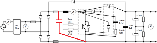
to summarise all the efforts from several of the treads this year (1, 2 and 3), I was finally able to get to higher DC voltages and powers without the 'noise' interfering with the serial communication. Thank you all who helped with advice and recommendations.
I have done the following:
- Used aluminium plates to connect DC-link capacitors instead of cables
- Added snubber capacitor and resistor (Csnub and Rsnub)
- Added output capacitor (Cout)
- Added SiC Shottky diode in parallel with IGBT chopper inverse diode
- Used SiC Shottky diode instead of the IGBT chopper forward diode
- Increased gate resistor values Rgon and Rgoff
- Increased serial communication baud rate
Pictures:
The first oscillogram shows input line current (Ch4, 10 mV/A), inductor output current (Ch3, 50 mV/A) and DC voltage (Ch2, 1/200 mV/V).
The second oscillogram is with the AC coupling for DC voltage
Both are recorded for Vout = 650 Vdc and Iout = 4.5 Adc (approx. 2.9 kW)
I still have some noise in the current signal, though. The frequency of that noise corresponds to the chopper switching frequency (20 kHz).
Not sure which, out of all seven, was The One that reduced the noise to an acceptable level and after which the communication didn't break.
Do you have any other suggestions for further improvements or this is good enough?
Thanks