urian
Full Member level 3
hi ,there
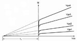
i want to find the channel modulation parameter λ in my process file to calculate the output resistance ro,but i dont know the name of it used in the process.
Then i download the BSIM4 model file and find that the Channel length modulation parameter is called PCLM.but i fail again to find it in my process file.
so anyone who knows the name of λ in common process file?
and how do you calculate the output resistance ro of a transistor?
by the way, the default value of PCLM in BSIM4 model file is 1.3, i think it is so large that i cant believe it is the so-called parameter λ.
regards
minci