Continue to Site

Welcome to EDAboard.com

Welcome to our site! EDAboard.com is an international Electronics Discussion Forum focused on EDA software, circuits, schematics, books, theory, papers, asic, pld, 8051, DSP, Network, RF, Analog Design, PCB, Service Manuals... and a whole lot more! To participate you need to register. Registration is free. Click here to register now.

About the center tap capacitor and resistor in IBM90nm

Status
Not open for further replies.

sendy

Newbie level 2
Joined
May 9, 2011
Messages
2
Helped
0
Reputation
0
Reaction score
0
Trophy points
1,281
Activity points
1,303
Hi All,

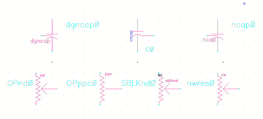
I am a newer for IBM 90nm process. In its PDK, the capacitors and resistors all have three terminals. I am just not sure how to connect the third terminal in the schematic, also in the layout.

Also, when I set up the capacitance value of the capacitor, I found we need to set up the length and width values and the software will give you the maximum and minimum capacitance value but not the exact capacitance value. How can I know if I set up the right capacitance value for the capacitor?


Could anyone tell me how to use those resistors and capacitors?

Thanks,
 

The top row could be variable capacitors. However the symbols do not match the traditional symbol which has an arrow going through the middle. The minimum and maximum values are its tunable range.

The bottom row is the typical symbol for potentiometers. Variable resistors.

Somewhere your application must have symbols for ordinary capacitors and resistors. 2 terminal type.

I have only a few 3-terminal capacitors scavenged from old circuit boards. They are two capacitors with one common pin. It doesn't have a unique symbol since it's electrically the same as two capacitors.
 

To be honest I did not use the IBM kit yet. But in general 3 terminals on caps are: + - and substrate under. The answer is in the model file. If you look into subcircuit definition in models you will find your answer.
Same thing for resistors - the model is using substrate connection because it usualy splits resistor to pi model C-R-C type device to model parasitics.
 

Teddy got it right, in IBM PDKs the third terminal is the well under the passive device and it is used to model parasitics.

I have used 130nm and 65nm and both show the value of the cap after setting geometry, make sure your PDK environment is in good shape, e.g, CXt file loaded in .cdsinit
 

I am just not sure how to connect the third terminal in the schematic, also in the layout.
connect to substrate potential

Also, when I set up the capacitance value of the capacitor, I found we need to set up the length and width values and the software will give you the maximum and minimum capacitance value but not the exact capacitance value. How can I know if I set up the right capacitance value for the capacitor?
dgncap and ncap are varactors not fixed capacitors.

i would advise you to use the MOSIS user group forum for this kit, and refrain from posting any specific information of a foundry process to a public forum as you are surely bound by an NDA with the foundry. **broken link removed**
 

connect to substrate potential


dgncap and ncap are varactors not fixed capacitors.

i would advise you to use the MOSIS user group forum for this kit, and refrain from posting any specific information of a foundry process to a public forum as you are surely bound by an NDA with the foundry. **broken link removed**

the third terminal is connected to the potential of the well under the device which is not necessarily substrate (it can be an nwell...)

dgncap and ncap are also designed to be used as decoupling caps
 

Status
Not open for further replies.

Part and Inventory Search

Welcome to EDABoard.com

Sponsor

Back
Top