Continue to Site

Welcome to EDAboard.com

Welcome to our site! EDAboard.com is an international Electronics Discussion Forum focused on EDA software, circuits, schematics, books, theory, papers, asic, pld, 8051, DSP, Network, RF, Analog Design, PCB, Service Manuals... and a whole lot more! To participate you need to register. Registration is free. Click here to register now.

A square wave generation from 600mv to 1.2v

Status
Not open for further replies.
Hello

I did use the DAC7611 with a PIC16f876A. It´s very precisious.

My project is to generate programmable wave form.

For low impedance output I used a operational amplifier (buffer).

Elio
 

Hello

I did use the DAC7611 with a PIC16f876A. It´s very precisious.

My project is to generate programmable wave form.

For low impedance output I used a operational amplifier (buffer).

Elio

but can we have an adjustable waveform from 600mv to 1.2 v without using any DAC but only using a Mcu...
 

no i get an offset voltage all the time....even the output goes high or low....

I was expecting this answer but I liked to hear it from you first, so that I can be sure I understood well your circuit.

Let us see from where this offset comes?

MCU pin is high:
In this state, we like the output voltage be at ground (0V). But to get it, the MCU supply voltage should be equal to or higher than the PMOS source voltage. Only if Vgs=0 (or positive), Id=0 (hence Vd=Vout=0 as well).
But in our actual circuit, the high state of the MCU pin is only 3.3V which means Vgs=3.3-5 = -1.7V hence, for most PMOS, the P channel starts to conduct and Ic is no more zero so we get an undesirable positive volt at Vd (Vout).

Before going on, may I ask:
Is it important to you to keep the two supplies be different for the MCU and PMOS?
In case they can be made equal, which one you prefer 3.3V or 5V?

The next solution will depend on your answer (no matter what will be).

Kerim
 

yes i am wrong ....but will this be enough to drive a PMOS??

Not with the fast timing you want, you can probably get 100-200ns, depends on the mosfet.
In general a schematic with specific components is very useful because anyone trying to help can easily see what is wrong.
For example your Pmosfet gate drive, you never shut down the mosfet because there is a Vgs in any state of the mcu, it would be clearly visible in a schematic but instead KerimF had to ask you 3-4 times to understand what you have done wrong.

Alex
 

Starting with the first post, you have disclosed your specification in little slices, so the question is, if my below compilation represents the complete specification?
a square wave with a frequency of 300-500HZ and the amplitude can be in the range of .6v - 1.3v
i would like to have an rise time and fall time that is very small ...may be 10 -20 nano sesonds
i need an 1.1vPWM signal as the output with 40ma current
expected output without any offset
can we have an adjustable waveform from 600mv to 1.2 v
If it is, the "adjustable waveform" feature (means amplitude, apparently) will surely restrict the design options. I also presume, that 27.5 ohm output resistance describes the intended behaviour correctly. In this case, a CMOS driver with variable 2.5 to 5 V supply voltage and a resistive 3:1 divider (110:36 ohm nominal) would meet the specification. Fast CMOS gates, possibly in a parallel circuit are well suited as a driver, better than discrete MOS transistors.

An adjustable output voltage can be most easily achieved by a variable resistor, of course.
 

I was expecting this answer but I liked to hear it from you first, so that I can be sure I understood well your circuit.

Let us see from where this offset comes?

MCU pin is high:
In this state, we like the output voltage be at ground (0V). But to get it, the MCU supply voltage should be equal to or higher than the PMOS source voltage. Only if Vgs=0 (or positive), Id=0 (hence Vd=Vout=0 as well).
But in our actual circuit, the high state of the MCU pin is only 3.3V which means Vgs=3.3-5 = -1.7V hence, for most PMOS, the P channel starts to conduct and Ic is no more zero so we get an undesirable positive volt at Vd (Vout).

Before going on, may I ask:
Is it important to you to keep the two supplies be different for the MCU and PMOS?
In case they can be made equal, which one you prefer 3.3V or 5V?

The next solution will depend on your answer (no matter what will be).

Kerim

yes i would like to prefer a 3.3 for both the source and the gate
 

yes i would like to prefer a 3.3 for both the source and the gate

Solution 1:
To use a PMOS transistor, it has to be selected based on its output characteristics (Id versus Vds) in order to satisfy the following (I will drop the sign for clarity):
For a value of Vds < (Vcc - Vout) = 3.3 - 1.1 = 2.2 V (actually Vds < 2 to have a margin), Id could be set as 40mA (assuming the load is 27.5 Ω or 27Ω) for a value of Vgs < 3.3.
I am not sure if you are able to decide on one PMOS (low power and based perhaps on some datasheets of the types that could be available to you). It will be easier to analyse and get numerical results after the selection of a specific PMOS. It is also important to consider the Id variation with the ambient temperature (and perhaps within the transistor during the start :wink: )

Solution 2:
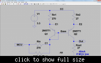
Instead of PMOS we can use a pnp transistor (also low power and fast enough, as 2N5771 for example). Please refer to the attached schematic. The use of Q1 (acts as a diode) is to decrease the temperature sensitivity of the circuit (its Vbe compensates to a good extent the variation of Q2 Vbe).

Kerim


Edited:
On the circuit, Roffset needs to be selected to get Iout as close to 40mA as possible. Obviously Rin and Roffset act as one resistor, so maybe they may be replaced by one resistor only as long you get the required output.
 
Last edited:
thanks kerim i will try this out schematic and will tell my results to you soon.....
 

Status
Not open for further replies.

Part and Inventory Search

Welcome to EDABoard.com

Sponsor

Back
Top