Continue to Site

Welcome to EDAboard.com

Welcome to our site! EDAboard.com is an international Electronics Discussion Forum focused on EDA software, circuits, schematics, books, theory, papers, asic, pld, 8051, DSP, Network, RF, Analog Design, PCB, Service Manuals... and a whole lot more! To participate you need to register. Registration is free. Click here to register now.

A question about p-n junction [hlp]

Status
Not open for further replies.

elec350

Full Member level 4
Joined
Dec 17, 2006
Messages
199
Helped
1
Reputation
2
Reaction score
0
Trophy points
1,296
Location
Iran
Activity points
2,548
Hello
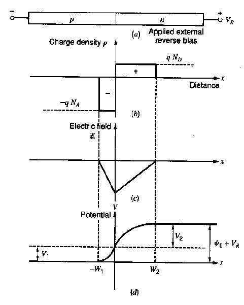
Below picture is from page 2 of Gray-Meyer's book. In part (a) of the picture, it is shown that the voltage VR is applied to p-n junction, but in part (d) the barrier potential is VR+Ψ0. Why? I have seen some of electronics book, but couldn't find the answer. pls hlp me.
27_1252076658.jpg
 

This is a very good question.

Fermi level for electrons (in n-type semiconductor) and for holes (in p-type semiconductor) are different. When n-type and p-type semiconductors are making a contact (to form a p-n junction), Fermi levels should become equal - that's the requirement for zero current flow (in steady-state or equilibrium condition, there should be no current). Equilibration of the Fermi levels is achieved by charging of the p- and n-type semiconductors - p-type is charged negatively, and n-type - positively. Thus, there is a potential difference between n- and p-type regions even when applied voltage V=0. The potential difference occurs in the depletion region around the metallurgical p-n junctions. The depletion region is where the charging of the semiconductors occur - and the charges are due to the ionized impurities not neutralized by the mobile carriers charges. The rest of the semiconductor (outside the depletion region) is electrically neutral.

The magnitude of the so-called built-in voltage (potential difference between n- and p-type regions) of the p-n junction is:

Vbi=kT/e*ln(NP/ni^2),

where kT/e is thermal potential (~25.8 mV at T=300K), N and P are doping density in n- and p-type regions, and ni is the intrinsic carrier concentration (~1e10 cm-3) at room temperature in Si).

Vbi is close to the bandgap (divided by electron charge e) - i.e ~1.1V in Si.

When external voltage V is applied to p-n junction (forward or reverse), it is added in addition to the buil-in voltage, so that the total potential difference between n- and p-type regions becomes: Vbi+V.
 

    elec350

    Points: 2
    Helpful Answer Positive Rating
I look at a biased pn-junction as one which gives an output voltage equal to the source voltage less the built-in voltage when forward biased and source voltage plus the built-in voltage when reverse biased. Of course the latter can be measured only with high imedance voltmeter because of almost zero reverse current.
 

ramdasravi said:
I look at a biased pn-junction as one which gives an output voltage equal to the source voltage less the built-in voltage when forward biased and source voltage plus the built-in voltage when reverse biased. Of course the latter can be measured only with high imedance voltmeter because of almost zero reverse current.

There is a lot of confusion over "potential difference" versus "voltage" - these two quantities are not equal to each other, in general.

"Potential difference" is the difference of the electrostatic potentials between two points (in this case - between the quasineutral regions of the p-n junction). Potential difference across un-biased (i.e. zero applied voltage) is Vbi. With applied bias V, potential difference is Vbi+V across the p-n junction (it gets bigger by absolute value for reverse voltage, and smaller - for forward voltage).

"Voltage" across p-n junction is the difference of the (quasi-) Fermi levels of electrons and holes in quasineutral regions. For un-biased p-n junction, voltage across p-n junction is zero. For applied voltage V, teh voltage across p-n junction is equal to V.

You can not measure potential difference across p-n junction using a voltmeter - what can be measured is the voltage across p-n junctions.
 

Status
Not open for further replies.

Similar threads

Part and Inventory Search

Welcome to EDABoard.com

Sponsor

Back
Top