Continue to Site

Welcome to EDAboard.com

Welcome to our site! EDAboard.com is an international Electronics Discussion Forum focused on EDA software, circuits, schematics, books, theory, papers, asic, pld, 8051, DSP, Network, RF, Analog Design, PCB, Service Manuals... and a whole lot more! To participate you need to register. Registration is free. Click here to register now.

a question about ADC grounding.

Status
Not open for further replies.

raychenchina

Newbie level 5
Joined
Sep 3, 2008
Messages
8
Helped
0
Reputation
0
Reaction score
0
Trophy points
1,281
Activity points
1,423
pcb adc grounding

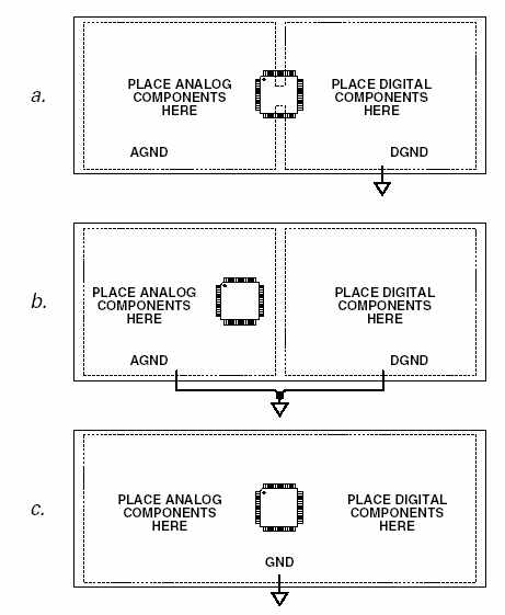
I have a question about ADC grounding. In the "Sensor Signal
Conditioning" published by ADI, the grounding is recommanded to
connect only in the power supply.
Also the ADC is regarded as analog device and is grounded to AGND.
My question is that if AGND and DGND is connected only in the power
supply, the current from DAC to buffer will flow through DGND - power
supply -AGND too. It's a big current loop, isn't it? Will it bring
noise to ADC's AGND?
Or I should use another ground method?

I can't upload the image, why?
 

adc grounding

Hi,
You separate Digital ground from AGND, coz usually digital gnd is more noisier than AGND. It is obvious since u hv swiching effect in digital electronics. If you connect DGND with AGND all the points u hv...u r virtually distorting your Analog signals...


Regards,
Shiva
 

You're right, that the suggested grounding scheme would inject the return current of the digital output into the analog plane. It's based apperently on the assumption, that this current is small compared to interferences generated internally in the two digital blocks. This assumption may be incorrect in some cases, e. g. for a fast parallel single ended ADC data output.

Thus the suggested grounding scheme shouldn't be understood as universal solution, to my opinion. ADI is discussing also different grounding schemes in other publications, e. g. in the ADuC836 data sheet:

99_1220431144.jpg


The present scheme is represented by variant b. in the drawing. Personally, I try to use variant c. in most systems (just a remark, don't want to discuss this in detail here).
 

i think that u need to connect the analog ground AGND with the digital ground DGND to minimize the noise coupling from the Digital to analog, while the return current flowing from the system analog to the system digital grounds will be the current of the interface logic of the ADC which should be minimized as much as possible
 

Mr Ott's opinion

Thank you all!
Did you read a review with Walt Kester? in the article below, I still can't find the answer how to connect AGND & DGND with power supply GND.

Q. I’ve read your data sheets and application notes and also attended
your seminars, but I’m still confused about how to deal with analog
(AGND) and digital (DGND) ground pins on an ADC. Your data
sheets usually say to tie the analog and digital grounds together at
the device, but I don’t want the ADC to become my system’s star
ground point. What do I do?
A. First of all, don’t feel bad that you are confused about what to
do with your analog and digital grounds. So are lots of folks!
Much of the confusion comes from the labeling of the ADC
ground pins in the first place. The pin names, AGND and
DGND, refer to what’s going on inside the component itself
and do not necessarily imply what you should do with them
externally. Let me explain.
Inside an IC that has both analog and digital circuits, such as
an ADC, the grounds are usually kept separate to avoid
coupling digital signals into the analog circuits. The diagram
shows a simple model of an ADC. There is really nothing the
IC designer can do about the wirebond inductance and
resistance associated with connecting the pads on the chip to
the package pins. The rapidly changing digital currents produce
a voltage at point B which will inevitably couple into point A
of the analog circuits through the stray capacitance. It’s the IC
designer’s job to make the chip work in spite of this. However,
you can see that in order to prevent further coupling, the AGND
and DGND pins should be joined together externally to the
same low impedance ground plane with minimum lead lengths.
Any extra external impedance in the DGND connection will
cause more digital noise to be developed at point B; it will, in
turn, couple more digital noise into the analog circuit through
the stray capacitance. Though an extremely simple model, this
serves to illustrate the point.


Q. O.K., you’ve told me to join the AGND and DGND pins of the IC
together to the same ground plane—but I am maintaining separate
analog and digital ground planes in my system. I want them tied
together only at one point: the common point where the power supply
returns are all joined together and connected to chassis ground. Now
what do I do?

A. If you have only one data converter in your system, you could
actually do what the data sheet says and tie your analog and
digital ground systems together at the converter. Your system
star ground point is now at the data converter. But this may be
extremely undesirable, unless you initially planned your system
with this thought in mind. If you have several data converters
located on different PCBs, the concept breaks down, because
the analog and digital ground systems are joined at each
converter on a number of PCBs. This is a perfect invitation for
ground loops!
Q. I think I’ve figured it out! If I must join the AGND and DGND
pins together at the device, and I want to maintain separate system
analog and digital grounds, I tie both AGND and DGND to either
the analog ground plane or the digital ground plane on the PCB,
but not both. Right? Now, which one should it be, since the ADC is
both an analog and a digital device?
A. Correct! Now, if you connect the AGND and DGND pins
both to the digital ground plane, your analog input signal is
going to have digital noise summed with it, because it is
probably single-ended and referenced to the analog ground
plane.
Q. So the right answer is to connect both AGND and DGND pins to
the analog ground plane? But doesn’t this inject digital noise on my
nice quiet analog ground plane? And isn’t the noise margin of the
output logic degraded because it now referenced to the analog ground
plane, and all the other logic is referenced to the digital ground plane?
I plan to run the ADC outputs to a backplane tristate data bus
which is going to be pretty noisy to begin with so I think I need all
the noise margin I can get.
A. Well, nobody ever said life was easy or fair! You have reached
the right conclusion by traveling a rocky road, but the problems
you suggest—digital noise on your analog ground plane and
reduced noise margin on your ADC outputs—really aren’t as
bad as they seem; they can be overcome. It is clearly better to
let a few hundred millivolts corrupt the digital interface than
to apply the same corrupting signal to the analog input where
the least-significant-bit for a 16-bit, 10-V-input-range ADC is
only 150 mV! First of all, the digital ground currents on DGND
pins can’t really be that bad, or they would have degraded the
internal analog parts of the ADC in the first place! If you bypass
the power pins of the ADC to the analog ground plane, using
a good-quality high-frequency ceramic capacitor for high
frequency noise (say 0.1 mF), you will isolate these currents to
a very small region around the IC, and they will have minimal
effect on the rest of your system.
You will incur some reduction in digital noise margin, but it is
usually acceptable with TTL or CMOS logic if it’s less than a
few hundred millivolts or so. If your ADC has single-ended
ECL outputs, you may want to put a push-pull gate on each
digital output—i.e., one with both true and complementary
outputs. Tie the grounds of this gate package to the analog
ground plane and connect the logic signals differentially across
the interface. Use a differential line receiver at the other end
which is grounded to the digital ground plane. The noise
between the analog and digital ground planes is now commonmode—
most of it will be rejected at the output of the differential
line receiver. You could use the same technique with TTL or
CMOS, but there is usually enough noise margin not to require
differential transmission techniques.

However, one thing you said troubles me greatly. In general, it
is unwise to connect the ADC outputs directly to a noisy data
bus. The bus noise may couple back into the ADC analog input
through the stray internal capacitance—which may range from
0.1 to 0.5 pF. It is much better to connect the ADC outputs
directly to an intermediate buffer latch located close to the
ADC. The buffer latch is grounded to your digital ground plane,
so its output logic levels are now compatible with those of the
rest of your system.


Q. I think I understand now, but why on earth didn’t you just call all
the ground pins of your ADC AGND in the first place; then none of
this would have come up in the first place?
A. Perhaps. But what if the incoming-inspection person connects
an ohmmeter between these pins and finds out that they are
not actually connected together inside the package? The whole
lot will probably be rejected—and the IC may be blown!
Furthermore, there is a tradition associated with ADC data
sheets which says we must label the pins to indicate their true
function, not what we would like them to be.
Q. O. K. Now, here comes a question I’ve been saving as your ultimate
test! I have a colleague who designed a system with separate analog
and digital ground systems. My colleague says that, with the ADC’s
AGND pin connected to the analog ground plane and the DGND
pin connected to the digital ground plane, the system is working
fine! How do you explain this?
A. First of all, just because a practice is not recommended doesn’t
necessarily mean you can’t get away with it some of the time
and thereby be lulled into a false sense of security. (This is one
of the lesser-known of Murphy’s Laws). Some ADCs are less
sensitive to external noise between the AGND and DGND
pins, and it may be that your colleague picked one of those by
accident. There could be other explanations—which would
require that we explore your colleague’s definition of “working
fine”—but the point is that the ADC’s specifications are not
guaranteed by the manufacturer under those operating
conditions. With a complex component like an ADC, it is
impossible to test the device under all possible operating
circumstances, especially those which aren’t recommended in
the first place! Your friend got lucky this time, but you can be
sure that Murphy’s law will ultimately catch up with him (or
her) if this practice is continued in future system designs.
Q. I think I understand the ADC grounding philosophy now, but what
about DACs?
A. The same philosophy applies. The DAC’s AGND and DGND
pins should be tied together and connected to the analog
ground plane. If the DAC has no input latches, the registers
driving the DAC should be referenced and grounded to the analog ground plane to prevent digital noise from coupling
into the analog output.
Q. What about mixed-signal chips which contain ADCs, DACs, and
DSPs such as your ADSP-21msp5O voiceband processor?
A. The same philosophy applies. You should never think of a
complex mixed-signal chip, such as the ADSP-21msp50, as
being only a digital chip! The same guidelines we’ve just been
discussing should be applied. Even though the effective
sampling rate of the 16-bit sigma-delta ADC and DAC is only
8 ksps, the converters operate at an oversampling frequency of
1 MHz. The device requires an external 13-MHz clock, and
an internal 52- MHz processor clock is generated from it with
a phase-locked loop. So you see, successful application of this
device requires an understanding of design techniques for both
precision- and high-speed circuits.
Q. What about the analog and digital power-supply requirements of
these devices? Should I buy separate analog and digital power supplies
or use the same supply?
A. This really depends on how much noise is on your digital
supply. The ADSP-21msp50, for example, has separate pins
for the +5- V analog supply and the +5-V digital supply. If you
have a relatively quiet digital supply, you can probably get away
with using it for the analog supply too. Be sure to properly
decouple each supply pin at the device with a 0.1-mF ceramic
capacitor. Remember to decouple to the analog ground plane,
not the digital ground plane! You may also want to use ferrite
beads for further isolation. The diagram below shows the proper
arrangement. A much safer solution is to use a separate +5-V
analog supply. You can generate the +5 V from a quiet +15-V
or +12-V supply using a three-terminal regulator, if you can
tolerate the extra power dissipation.


Added after 2 hours 14 minutes:


http://www.hottconsultants.com/techtips/split-gnd-plane.html

In Mr Ott's opinion, the ground should be partitioned not split. For your information
 

Status
Not open for further replies.

Part and Inventory Search

Welcome to EDABoard.com

Sponsor

Back
Top