Continue to Site

Welcome to EDAboard.com

Welcome to our site! EDAboard.com is an international Electronics Discussion Forum focused on EDA software, circuits, schematics, books, theory, papers, asic, pld, 8051, DSP, Network, RF, Analog Design, PCB, Service Manuals... and a whole lot more! To participate you need to register. Registration is free. Click here to register now.

A question about 6N136

Status
Not open for further replies.

kappa_am

Full Member level 6
Joined
Jul 16, 2012
Messages
331
Helped
19
Reputation
38
Reaction score
19
Trophy points
1,298
Location
Vancouver
Activity points
3,859
Hi all,
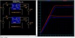
I am designing a circuit in which I have to use 6N136 with Vcc=15v. The TPHL ( delay time from high to low logic on output) and TPLH(delay time from low to high logic on output) are very important for me, but in the datasheet the curves are drawn in Vcc=5V. I like to know how these curve changes by changing Vcc form 5v to 15v. the behavior of curves in Fig.3, Fig. 5 and Fig. 6 are important for me.
The datasheet can be accessed by following link:
https://www.fairchildsemi.com/ds/6N/6N136.pdf

I would be grateful if you share your Idea.
 

The TLH and THL are both dependant on collector current, voltage slew rate, capacitive load of 1.5uF in Figure 7, resulting slew rates and Vcc. Thus you may need to reduce load cap. to compensate for 3x voltage, Vcc. since your Rc will need to be increased 3x to maintain same current.

You must define your requirements and use worst-case tolerances on CTR for selected drive and load current to estimate dv/dt , to reach switch threshold on target device and latency.
 

Some of these curves are already defined to IF at range of 10-16mA, but increasing the supply from a factor of 3x would also multiply IF to something staying much above device limit of 25mA.
 

according to maximum current that my MCU can provide I have to choose IF=10mA, maximal. I need that TPLH be lower that TPHL more than 400ns, not longer than 800ns. in Fig. 3 of the datasheet with IF=10ma at Vcc=5V, Io=3.7ma,approximately. first question is increasing VCC form 5v to 15v, how affect this curve while If is constant.
the second question is about fig. 7, will I have same curves if I increase RL and reduce CL 3 times? or affect of changing VCC on this curve is nonlinear?

Thank you

- - - Updated - - -

Some of these curves are already defined to IF at range of 10-16mA, but increasing the supply from a factor of 3x would also multiply IF to something staying much above device limit of 25mA.

The supply on the Diode side is 5v, it supply by MCU. using a 330 Ohm in series with diode limits the IF to roughly 10mA.
 

What properly define the conduction region of these passive opto devices on its characteristic curve is the current flowing through the inner input/output components regardless external voltage supply used, therefore for the same IF current, defining different biasing RL resistors to produce the same output current using 5v and 15v supplies would produce the same result in both cases. The only change, indeed is the fact that for 15v the output would reach faster and overflow a high TTL logic level, if compared to the original 5V.

Biasing the input diode with 10mA instead 16mA, the output current at transistor collector will not corresponds anymore to the 3,7mA after 4.0u seconds but something near to 2,1mA after ~6.0u seconds whichever the RL selected,what means reducing the current at input side, increase significantly the propagation time:
 

Attachments

  • 6N136.JPG
    6N136.JPG
    86.6 KB · Views: 61

Dear Andre, thank you for your reply.
According to the Fig. 3 in the datasheet, when IF=10mA and Vo= 15v, The output current should be 4mA; since according to your answer change of Vcc has no effect on curves when IF and Io are kept unchanged. Propagation delay is also obtained from Fig. 6. I think if we put Rf=330 Ohm and Rout= 3.3K ohm the difference of the TLH and THL would be about 200ns. please confirm.
I am little bit confused the result of the simulation which you have attached is different of those indicated in datasheet.


Thank you
 

You´re right, there is a possible problem either on the model or simulation parameters.

Anyway, disregarding results above, we can take the conclusion that in order to increase the transfer speed, the IF current must rise, so why don´t you connect 2 Microcontroler output pins - working together - to improve the current source capacity from 10mA to 20mA ?

Another point is that for an application involving a more demanding speed requirement, considering that you´re already using different sources at each side, probably would be more suitable you employ some active opto, due it have best performance on speed features.
 

as long as propagation delay is below 1.5us, it is out of concern. Having 400ns<THL-TLH<800ns is my main desire. I was thought I could reach this by IF= 10mA. To have IF=10mA I have to use 330 Ohm resistor in series with diode side. looking to Fig. 3 when IF=10mA and Vo=15V, Io should be 4mA ( I am not sure about this because these curves are drawn with Vcc=5v, while in my project Vcc=15V). Vo=15v so to have Io=4mA the Ro has to be approximately 3.9K Ohm that by Fig. 6 THL-TLH=130ns. this does not fulfill requirements. to fulfill the requirement, I need Ro=2.2K ohm that means Io=6.8mA and If=16-17mA (please confirm). but MCU problem is raised in this situation.
Do you know a opto coupler that has THL longer than TLH?
 

Do you know a opto coupler that has THL longer than TLH?

Generally these parameters are informed on parametric search tools as having the same value or THL>TLH, but not the opposite, and don´t know the technical reason. Anyway, once you are apparently dealing with severe speed transfer requirements, why don´t you consider use some opto coupler based on active device as for instance this here ?

https://www.mouser.com/ds/2/38/V02-2947EN_DS_ACPL-M484_2013-09-23-256503.pdf
 

For an optocoupler, a simple and straightforward means of speeding up the output is to employ a cascode connection.

I'm typing from my phone and can't draw a circuit. Google the term.
 

For an optocoupler, a simple and straightforward means of speeding up the output is to employ a cascode connection.

Seems as this option probably may be more sensitive to noise, but I may be wrong. I presume an opto circuit based on active device, due to have high gain circuit inside already biased, the propagation time tend to be somewhat reduced.
 

Thank you for your reply; I looked at the link, but as I state before, I am not looking for very fast Optocoupler. indeed a delay up to 2us may be tolerated. The main requirement is an difference between TPHL and TPLH larger than 400ns and less than 800ns (400ns<TPHL-TPLH<800ns).
Exhausted by checking many datasheets and solution guides!! :(
another question is in some datasheets the condition of checking Ton and Toff is strange. For example TLP 521; the test condition is Vcc=10V, Ic=2mA R=100 ohm, when Opto is on the output will be 9.8V and when it is off it will be 10V. I have seen this condition in many datasheet. why they test the Optos in not-saturated condition for indicating toff and tON, while the output does not mean on or off logically?

Thank you

- - - Updated - - -

Generally these parameters are informed on parametric search tools as having the same value or THL>TLH, but not the opposite, and don´t know the technical reason. Anyway, once you are apparently dealing with severe speed transfer requirements, why don´t you consider use some opto coupler based on active device as for instance this here ?

https://www.mouser.com/ds/2/38/V02-2947EN_DS_ACPL-M484_2013-09-23-256503.pdf

I found some optocoupler that have tOn longer than toff for example MOC213M but the test condition is not in saturated condition. it is tested at IC=2ma, Vcc=10v, RL=100 ohm!!! the difference between Vo in ON and OFF states is roughly 0.2V!
I am wondering why they tested toe component in this condition!!
 

The main requirement is an difference between TPHL and TPLH larger than 400ns and less than 800ns (400ns<TPHL-TPLH<800ns)

I guess that putting a proper Resistor/Capacitor/Diode net before the opto input forward diode you could thereby add a unequal delay to the rising or the falling edge ( you should select some ultra-fast diode ) so that could compensate the difference of TPHL and TPLH.
 

So far we considered the source of the trigger as an ideal voltage source so as to not foresee the contribution of any additional delay from the output of the uC, nor the temperature variation in the THL and TLH whose effect would certainly not be symmetrical .

Such a demanding requirement like that can probably only be calibrated by an additional net empirically during assembly adjustments , so that the reproduction in large scale may be impractical.
 

Thanks, I think the extra-circuit idea sounds good and worth to try. However, I think designing such a circuit is somewhat difficult because of non-idealities.
 

Theoretically, something like this should suffice:

RCD.JPG
 

Status
Not open for further replies.

Part and Inventory Search

Welcome to EDABoard.com

Sponsor

Back
Top