Continue to Site

Welcome to EDAboard.com

Welcome to our site! EDAboard.com is an international Electronics Discussion Forum focused on EDA software, circuits, schematics, books, theory, papers, asic, pld, 8051, DSP, Network, RF, Analog Design, PCB, Service Manuals... and a whole lot more! To participate you need to register. Registration is free. Click here to register now.

a problem with my power mosfets/capacitor cahrging

Status
Not open for further replies.

elahetal

Junior Member level 1
Joined
Jul 21, 2010
Messages
15
Helped
0
Reputation
0
Reaction score
0
Trophy points
1,281
Activity points
1,406
Hello Guys,

I have some problem and I really appreciate if you have a look at my circuit.Any comments, ideas, solutions,....are really appreciated!

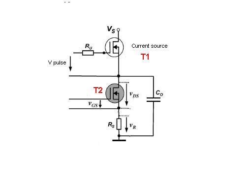
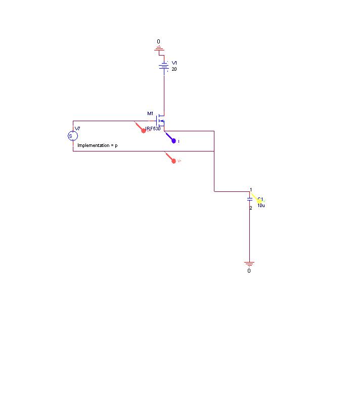
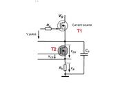
I have a circuit like Fig.1

The theory is:

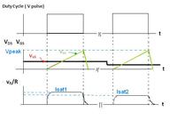
The upper MOSFET gate is driven to active region by very short pulse width (not less than 300us) and low frequency or single pulse.
It is supposed to act as a current source to charge the capacitor across the power MOSFET.

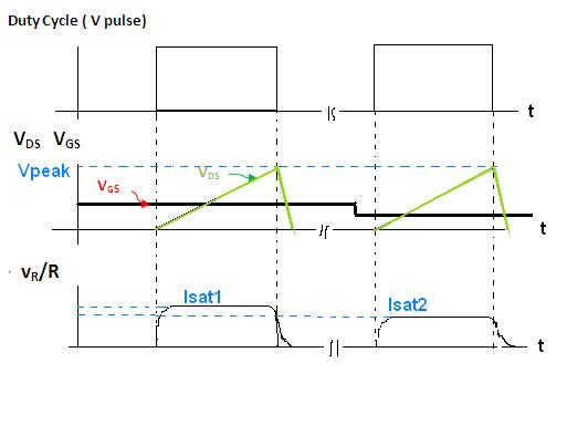
After the gate voltage is established in T2, T1 is driven to active region to act as a voltage controllable current source to provide constant current (I). Thus, the voltage vDS across the T2 increases in a linear fashion as C0 is charging with the constant current I. The drain current of T2 rises until it reaches saturation. T1 is then turned off slowly when the voltage vDS reaches the maximum allowed voltage (Vpeak). Then, the reverse operation occurs i.e. the voltage across C0 discharges through the channel of T2 toward zero. Fig. 2 shows the operation diagram.
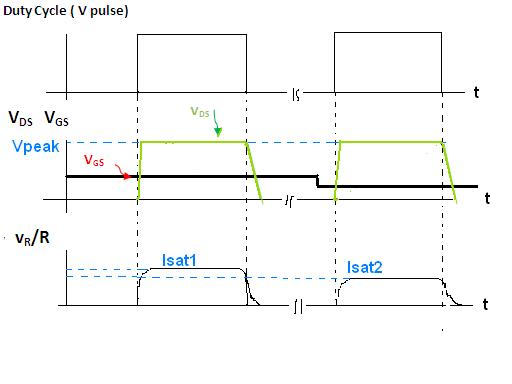
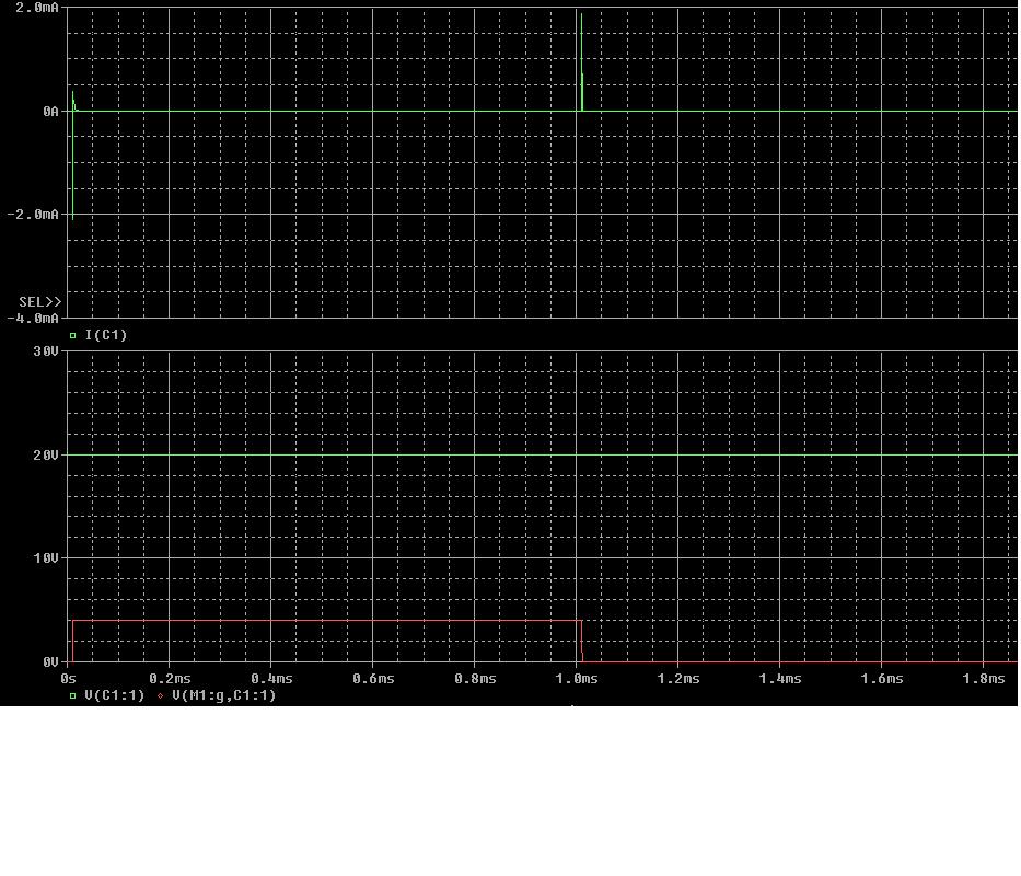
But what I see is the results in Fig 3.
( I have the same results both experimentally and PSpice simulation)


I am sort of puzzled by your circuit because T1 is an NMOS source follower, not a current source, unless I have missed something. So, the charging would be rapid, as would appear to be the case. Did you intend T1 to be a PMOS?

Keith.
 

Hi keith, No it is NMOS and intended to work in active region(always)....then it would work as a current source....
You believe it should be a Pmos if I want it to work as a current source?
 

Well, an NMOS source follower isn't a current source so the results you are getting are the results I would expect. A PMOS connected common source can be a current source if you drive the gate voltage to the correct level (but the gate voltage logic would be inverted).

Is this for integration on a custom IC or to be made from discrete parts?

I am not sure what you are trying to achieve. Well, I can see the waveforms you want, but I am not sure why. Also, I don't have a feel for the voltages and currents involved i.e. a few volts or hundreds, a few mA or tens of amps.

Also, I guess, the speed involved. You mention 300us (not really "a very short pulse") but that would make the period of the signal in the millisecond region, I would have thought.

With a bit more information I will try to help.

Keith
 

    elahetal

    Points: 2
    Helpful Answer Positive Rating
Thanks a lot Keith,

It is made from discrete parts so I can choose my components(MOSFETs and gate driver) individually.

What I am looking for is to see the slope when charging the capacitor.In other words, the Mosfet in parallel with capacitor is my DUT and I intend to stimulate its drain-source with voltage slope(when the C is charging) ....so it is important to control the slope...
my DUT is a high current MOSFET(max 110A) but low voltage(max 15v).
Your assumption about period is completely right..the period will be around milliseconds BUT I may have to use single pulses as well.
To wrap up, I want to make a voltage slope by charging the capacitor and the slope should be controllable.

I tried to answer your questions..if you need more info..I will be glad to provide and really really thanks for following up.

Added after 5 hours 40 minutes:

HI Keith,

I simulated my circuit is pspice using Pmos for current source but the result is the same ...I can't see the slope.....
I'm in need of help guys....please....
 

You can do it with an NMOS but it requires a floating pulse voltage between the gate and source oft he NMOS. I have attached what I mean. It is not a good circuit - the voltage to drive the NMOS gate needs to generate a fixed voltage between the gate and source which means the gate voltage has to increase as the capacitor charges.

Using a PMOS is slightly easier because you only need to pulse the gate relative to the positive supply - it doesn't have to float. However, both methods are poor as they rely on precise MOSFET characteristics to set the current. These will vary from device to device and with temperature.

An improved circuit would add a resistor to the source of a PMOS. This will lose you some supply voltage but give a little stability to the current with temperature changes. I have attached an example.

The best way is to use an opamp and a resistor in the PMOS source and use that to control the gate. I have tried to illustrate the idea. Don't copy it - I am short of time at the moment so copious amounts of cheating have been used. You need an opamp which can work with an input at the positive rail - I have cheated with the power supply.

Keith.
 

Thanks a lot Keith for your help.

The problem is that, I have used high-side gate driver to make a floating point but , when the T1 turns off the capacitor charges through the boot strap capacitor instead of discharging through the channel of T2,in addition, again I can not see the slope....I'll give a try by opamp in spice and let you know...maybe I make some mistakes while simulation....anyway really thanks Keith
 

Hi Keith,

I simulated the Pmos circuit..that works...the same as your file but the problem is that when I place a parallel mosfet with the capacitor the current is very low....

I got the slope by NMOS as well(practically, not in simulation) but I have the same problem....
I mean when I adjust the upper mosfet for current source about 10A and set the lower MOSFET VG for the same current , the current I see practically is about 1A...do you have any idea why?
 

I don't understand your description of what is happening.

So you set it for 10A charge current and 10A discharge current? You turn off the charge current and turn on the discharge and only see 1A not 10A - is that what you are seeing?

Maybe a simulation showing it would help me understand the problem.

Keith.
 

Hi Keith,

Thanks for your help, I really appreciate that.
leave aside what I said, I solved that problem about PMOS.

Talking about NMOS that You sent me, I can't get those waveforms, I attach the result.


You need an "initial condition" on the capacitor so it starts off at zero volts - yours starts at 20V. I am not sure how you do that in your simulator. Another solution would be to put a large resistor across the capacitor to counteract the MOSFET leakage. 10meg should do it.

Keith.
 

    elahetal

    Points: 2
    Helpful Answer Positive Rating
I agree with keith, you do need to set the IC in pspice for the cap to zero. Double click on the cap in pspice and in the properties there is an IC box. Change the value to 0V. I would also add that you will not see the slope of the charge since you are using a perfect capacitor and a perfect power source. There is no impedance except the small Rdson of the fet. Remember t(tau) = R*C. So, if you want a specific rise time of voltage on the cap you need to add a resistor in series with the cap. You should probably add a gate resistor to the fet to slow down the turn on time.
 

The circuit idea (not without its flaws) is to use the NMOS as a constant current source which will result in the linear ramp. See my earlier post.

Keith.
 

Status
Not open for further replies.

Part and Inventory Search

Welcome to EDABoard.com

Sponsor

Back
Top