JackLin063
Newbie
Hi,
I'm currently designing CDAC. I have some questions about capacitor voltage division.
In Figure 1, this is the test bench for simulating capacitive voltage division. All capacitors are ideal capacitors with a capacitance of 1pF.
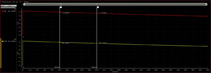
Figure 2 shows the waveforms of VO and VO2. I would expect VO and VO2 to be about 1/2*VREF, but the voltage will drop over time.
Here are my questions :
Q1. Is it the leakage of the mos switch that causes the VO to drop over time?
Q2. I'm using an ideal switch (W0 and W1, please refer to Figure 1) with an Open switch resistance of about 1T Ohms and a Close switch resistance of about 1 Ohms.
Why does the voltage of VO2 still drop over time? (My opinion is, an ideal switch has no leakage and the voltage VO2 should not drop over time)
Thank you in advance

I'm currently designing CDAC. I have some questions about capacitor voltage division.
In Figure 1, this is the test bench for simulating capacitive voltage division. All capacitors are ideal capacitors with a capacitance of 1pF.
Figure 2 shows the waveforms of VO and VO2. I would expect VO and VO2 to be about 1/2*VREF, but the voltage will drop over time.
Here are my questions :
Q1. Is it the leakage of the mos switch that causes the VO to drop over time?
Q2. I'm using an ideal switch (W0 and W1, please refer to Figure 1) with an Open switch resistance of about 1T Ohms and a Close switch resistance of about 1 Ohms.
Why does the voltage of VO2 still drop over time? (My opinion is, an ideal switch has no leakage and the voltage VO2 should not drop over time)
Thank you in advance