Continue to Site

Welcome to EDAboard.com

Welcome to our site! EDAboard.com is an international Electronics Discussion Forum focused on EDA software, circuits, schematics, books, theory, papers, asic, pld, 8051, DSP, Network, RF, Analog Design, PCB, Service Manuals... and a whole lot more! To participate you need to register. Registration is free. Click here to register now.

a low voltage ZTAT current generator

Status
Not open for further replies.

cmos_ajay

Full Member level 2
Joined
Jan 30, 2007
Messages
126
Helped
0
Reputation
0
Reaction score
0
Trophy points
1,296
Activity points
2,247
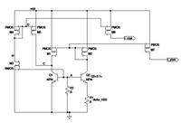
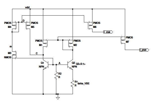
The attachment is a CTAT and PTAT current generator circuit for low voltage operation. My understanding is that as temperature increases, the Vbe(Q1) decreases and Id5 decreases since Vbe / R2 has decreases. This generates the CTAT current. Combination of the CTAT and PTAT currents makes a ZTAT current which is quite good.

However, my understanding of the role of devices M3, M4 (diode connected) and M5 is not so clear. I feel that these devices try to hold the Vcb (Q1), the collector base voltage as constant. Suppose, voltage at node A increases, then the voltage at node B decreases since M3 is like a common source device. Hence the current in M4 and M5 increases and voltage at node C increases. So the voltage at node A reduces and comes back to its original value.

Is my explanation of this feedback action correct or is there any alternative explanation ??

** This circuit is on page 425 of the book CMOS analog circuit design - Allen and Holberg (2nd edition)
 

Buddy, I guess you drew the schematic uncorrectly, pls check it out by comparing exactly with fig 7.6-15 on page 425 from Allen's book first :)

Your understanding is right. But you'd better explain from the current perspective using feedback. In Fig 7.6-15 on Alllen's book, you will see that the current flowing out of M8 is the one that flowing on R3(ignoring the base current of Q1 & Q2). But what if IDS8 is not the same as Vbe/R3? It's possible because M8 acts like a current source whose current is not determined by the voltage drop on R3 but the current from M7(mirroring effect). Without M8, the current flowing on R3 is also Vbe/R3. The two currents are definitely independent with each other. So any mismatch about the two currents between M8 and Ir3 is tranlated into the potential change on the BJT base terminal. Using some loop (negative feedback loop) to sense this change will give rise to the stablization of DC points of the circuit, i.e., current flowing though M7 M8 and R3 must be the same, which is Vbe/R3.

I hope it's helpful.
 

Thanks for the explanation. If you refer to the original paper ' A 1.1V current mode and piecewise curvature corrected bandgap reference' by P Allen and Rincon-mora (figure 4), there are R and C stabilizing components.
* Where do I cut the loop to determine stability and how to do this in Cadence ?
* How do I determine R and C values ?
Regards.
 

I've read this paper before but I cannot find it. Would you pls attach the pdf format file here?

* You can cut the loop anywhere by inserting iProbe element from analogLib library and perform the stb analysis to see the phase margin, gain margin and GBW to test the stability of the negative feedback loop.

* I don't remember where the RC located in this paper, but I guess the function of the two device is to perform frequency compensation. Maybe it's just some parallel compensation not miller compensation. Show me the schematic please. You should estimate the dominant pole and first nondominant pole and choose the RC value to make the first nondominant pole out of the GBW of the loop. This could be seen in the stb analysis.
 

Hello, The paper is available for free at the author's website.
**broken link removed**

I am not supposed to attach a IEEE paper on this site as per their rules. So the link will be useful.
Regards.
 

Hello, The paper is available for free at the author's website.
**broken link removed**

I am not supposed to attach a IEEE paper on this site as per their rules. So the link will be useful.
Regards.

Well, it's obvious that the RC form the Miller Compensation. So just follow Allen's hint given in the two-stage OPAMP design chapter in his famous book to calculate the exact values of the two passive devices(R is used as RHP zero-cancellation device). Note that in order to utilize Miller effect effectively, Miller compensators are always placed by shunting the input and ouput of the gain stage in the loop, such as the bjt in common emitter configuration.
Don't forget to perform the stb analysis to test the loop stability. Maybe it would be a trial and error process.
 

I saw the frequency response 'without compensation'. It shows the presence of a zero in the LHP near the dominant pole and is stable system. The phase margin was poor though. I tried the Miller compensation, which improved the phase margin and gain margin. But its not possible to get rid of that LHP zero which is below the unity gain frequency. Any suggestions ?? Thanks.
 

When I cut the loop at the gate of the M3 and insert iprobe, (refer to my schematic attached in the above post), I do not see that LHP zero after RC compensation is added. The response is good.
But if cut it at the base of Q1, then I see the LHP zero before f_unity and also a double pole.
What is the correct place to cut the loop ??
 

Status
Not open for further replies.

Part and Inventory Search

Welcome to EDABoard.com

Sponsor

Back
Top