karthik2dave
Newbie level 5
anybody know how to find 90 degree traces in pcb soft wares once finished routing... like as allegro, pads layout etc... if any found script please provide
Follow along with the video below to see how to install our site as a web app on your home screen.
Note: This feature may not be available in some browsers.

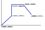
X0000000Y0000000…
X1111111Y1111111…
X1111111Y2222222…
X2222222Y2222222…
X2222222Y1111111…You don't route with a D code, that is down to the plotting, and you NEVER draw with a square D-code ever, even when we had to put the apertures in the aperture wheel we never used a square aperture.
There are many papers and comments on 90 degree corners including Howard Johnsons view, I don't use them because I don't think the boards look pretty enough when they are used, but have done to prove a point and don't worry if one or two appear on a board.
Then if your signal goes through a via the it travels through 2 right angled bends.....
It is possible to create a simple program in some high level language ( e.g Java ) that opens the output ASCII generated Gerber text file to seek for orthogonal coordinates at subsequent positions. In other words, if some two consecutive track are defined as
- <Pi ,Pi+1> = <(XiYi),(Xi+1Yi+1)>
- <Pi+1 ,Pi+2> = <(Xi+1Yi+1),(Xi+2Yi+2)>
We can assume that both tracks have a 90 degree rotation either if :
- Xi=Yi+1 and Yi+1=Xi+2 or
- Yi=Xi+1 and Xi+1=Yi+2
With a simple string manipulation, this should be not too difficult to scan the entire board. Knowing that the standard EIA RS-274 pattern that defines traces is something like formatted bellow:
Therefore, at the above sample we can note that the angle at the corner between traces <(111111,11111),(11111,22222)> and <(222222,22222),(22222,11111)> is orthogonal. The only remark on this approach is that such technique do not provide a friendly way to graphically interface with the user, being necessary a further interaction with the original CAD to find the matching corner.Code:X0000000Y0000000… X1111111Y1111111… X1111111Y2222222… X2222222Y2222222… X2222222Y1111111…
")
anybody know how to find 90 degree traces in pcb soft wares once finished routing... like as allegro, pads layout etc... if any found script please provide