Continue to Site

Welcome to EDAboard.com

Welcome to our site! EDAboard.com is an international Electronics Discussion Forum focused on EDA software, circuits, schematics, books, theory, papers, asic, pld, 8051, DSP, Network, RF, Analog Design, PCB, Service Manuals... and a whole lot more! To participate you need to register. Registration is free. Click here to register now.

what is 0.18u and 036u tech and differences

Status
Not open for further replies.

gbaerf

Full Member level 2
Joined
Aug 29, 2005
Messages
143
Helped
8
Reputation
16
Reaction score
1
Trophy points
1,298
Location
belongs to whole word
Activity points
2,295
I have posted the same in another questions as well....but for better clarity I am putting some other questions as well..
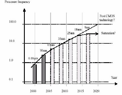
what do mean by 0.18 micron and 0.36 technology???
how thsese two arte different ????
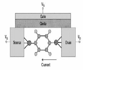
does the 0.18 is transiter width or length of the channel????
which one is latest technology running now a days????

complexity of chip is increasing and transister size is reducing so now a days
width of the transiter or channel lenght goes into nanometer...Am I right or not
 

ya you are right.

.18u meter technology means the distance between the source and the drain is .18u meter. similarly the others.

since gm is inversely proportional to the length, and gm is ditectly proportional to the bw of operation, shorter lengthed channels are preffered. however the channel length modulation effects are terribly more pronounced in short lengthed channels.

however upto my knowledge the current technology is 45 nano meter.

regards,
 

ok so telling you in brief a technology node is a minimum width of a line that can be drawn on a silicon....that is for .18 micron the minimum value of length or width or for that matters wire width can not be smaller then 180 nanometers......but usually length is kept minimum and varying the width of trasistor,so many people also say that length of transostor is .18 micron


for current technology 32 nano is in research right now.that is a width just enough to accomodate two silicon atoms between source and drain......such is the compactness that we have reached.......hope u'll benefit from this info.
 

It represents gate length.

L=0.18µ / 0.36µ

Ciao
 

feature size of channel length.
basic point you need make it clear when I decide to jump in this industry
 

Hellow amriths04,

means according to you 0.18u is distance between source and drain ..means it is the lenght of the channel......
Than what about the width Does 0.18u is not at all related to width of the channel.
what do u say about this....

regards/gbaerf
 

Dear gbaerf,

the min. width u can draw is dependent on the design rule provided in the technology, if u want to find that then draw a layout of a transistor and check the DRC

Regards
 

90nm is std upto date .


Feature transistor


Added after 4 minutes:

recently 10nm transistor is realized separately
 

65nm 2007
 

Status
Not open for further replies.

Part and Inventory Search

Welcome to EDABoard.com

Sponsor

Back
Top