Continue to Site

Welcome to EDAboard.com

Welcome to our site! EDAboard.com is an international Electronics Discussion Forum focused on EDA software, circuits, schematics, books, theory, papers, asic, pld, 8051, DSP, Network, RF, Analog Design, PCB, Service Manuals... and a whole lot more! To participate you need to register. Registration is free. Click here to register now.

74HC595 (shidt register) data output is out of phase with clock

Status
Not open for further replies.

myle00

Newbie level 5
Joined
Sep 30, 2010
Messages
8
Helped
0
Reputation
0
Reaction score
0
Trophy points
1,281
Location
U.S.A.
Activity points
1,432
Hi,

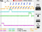
I'm trying to connect multiple 74hc595 shift register in series so that I can get more than 8 bits output. The problem is that the data output of the first shift register, which is supposed to be the data input to the second sr, is early by half of a clock cycle relative to the input data. The attached scope picture shows what I mean. The yellow (ch1) line is the clock signal that I generate. The blue line (ch2) is the data that I send to the first 74hc595. The green line (ch4) is the data output that I'm supposed to use as the input for the next shift register. However, because it's early by a half cycle relative to the clock, the data output on the second shift register is wrong.

To be more precise, the output (ch4) data line, is supposed to delay the input data line (ch2) by 8 clock cycles, but from the image you can see it's delayed by only 7.5 cycles, which brings that out of sync.

The device that outputs these signals to the shift register is either an FT232 or an FT2232H (used for the picture attached), both in bit bang mode. It's weird because from my identical boards using this shift register, some have this problem while others don't. I suppose the issue is because of some impedance mismatch, but I don't know how to solve it. I do place filtering capacitors (0.1uF) at VCC.

Thanks,
Matt
F0003TEK.png
 

I assume that you are using the Q7' output (pin 9) of one chip to feed serial in of the next?

The Q7' (with an apostrophe) as opposed to Q7 (no apostrophe)

Maybe you could tell us which trace colour on the scope corresponds to which pin of 74HC595
 
Last edited:

The cause of the error is that you provide the data synchronized on falling edges while the shift register operates on rising edges.
 

The captured diagram is correct. To have exact 8 clocks delay you need a input signal synchronous with shift clock.
74HC595 shift data on rising edge of clock, so the output signal cannot start on falling edge (like the input).
 
  • Like
Reactions: myle00

    myle00

    Points: 2
    Helpful Answer Positive Rating
Interesting how the Philips datasheet shows completely different signal names to the On-semi one. At least the pin numbers match up.

Just to be clear - pin 9 of the first chip goes to pin 14 of the next?
 
Last edited:

I measure 8 rising edges , I don't understand what you mean by 7.5 clocks

74hc595.jpg
 
  • Like
Reactions: myle00

    myle00

    Points: 2
    Helpful Answer Positive Rating
Interesting how the Philips datasheet shows completely different signal names to the On-semi one. At least the pin numbers match up.

Just to be clear - pin 9 of the first chip goes to pin 14 of the next?
Correct.

I measure 8 rising edges , I don't understand what you mean by 7.5 clocks

Ohh, you're right. You were counting + edges in which you're correct that there's 8. But I was counting from when I first output the data line to high which was when the clock was low. So counting 1 low+high as a single cycle, the output was shown at 7.5 cycles. But I get it now that I was counting wrong and that this is how the graph is supposed to look.

Anyway, my problem now is that when I did connect the output (SQh) of the first sr to the input of the second (whilst using the same clock fed to both), in some of my boards the output data line (SQh) must have been ever so slightly late because the data wasn't output properly. In other words, it seemed that SQh wasn't outputing fast enough to arrive in time for that 8th + edge. And for the same type of board some had this problem while others worked perfectly. Is there something I can/need to make it work robustly?

Thanks,
Matt
 

Your clock frequency is about 250KHz ?
Maybe you get the wrong data becasue you are entering data on falling edges, can you use rising edge logic?
 

The cause of the error is that you provide the data synchronized on falling edges while the shift register operates on rising edges.
@alexan_e Are you sure that there is a problem here?

Data changing on a falling clock seems like a good idea, as it will be stable on a rising clock, when it is read.

The scope traces for Clock and data input seem to me to tie up with the Philips datasheet timing diagram. I do not trust the On-semi datasheet, which looks to me to have errors.

The green scope trace does not match up with the Philips datasheet timing diagrams. The green trace looks wrong to me, as the data changes on the rising edge - which will mean that the next chip will clock as data is changing.

I cannot make sense of the evidence I see in this thread, but maybe I am just not thinking hard enough.

@myle00 Are you scoping on the 74HC595 pins? and are you sure that you do not have "invert" selected on any scope channel?

---------- Post added at 22:38 ---------- Previous post was at 22:17 ----------

I agree with the OP's assessment in the title of this thread.

If the scope traces are an accurate representation of the signals on the 74HC595 pins, then there seems to be something badly wrong.

If the input of the first chip changes on falling clock (so it is stable on a rising clock), then the input to the second chip should change on a falling clock.

The green trace (if accurate) is the source of the second chip's data input, so I would think it should change on falling clock - but it does NOT.

I cannot explain it.
 
Last edited:

I don't see a point of entering the data on falling edge, as you have already noticed the data in the output to the second chip (and the rest) will be on rising edge so you can't keep that falling edge timing.

---------- Post added at 00:41 ---------- Previous post was at 00:39 ----------

The shift register works on rising edges, this will not change because you want to enter data on falling edges.
Both input and output process data on rising edge.
I agree that it does not matter if data is changed at some time other than falling edge, but surely it is vital that data does NOT change exactly on a rising edge, which is what the green scope trace does.

I cannot see what is wrong with the clock and data input (yellow and blue traces). They look good to me.

---------- Post added at 23:04 ---------- Previous post was at 22:51 ----------

OK - apology time!

I have zoomed out a bit on my Philips datasheet, and I now see that I am confusing shift clock with store clock.

The scope traces seem to fit the Philips datasheet timing diagram perfectly.

I reckon the Op's circuit is operating exactly as it is supposed to, going by the scope traces.

Still leaves the original problem of intermittent operation though.

The particular chip I use is rated up to 57MHz, so 250KHz does not sound too taxing, as long as the connecting wires/traces are not overly long.


Sorry for getting it wrong!
 

If the scope traces are an accurate representation of the signals on the 74HC595 pins, then there seems to be something badly wrong.

If the input of the first chip changes on falling clock (so it is stable on a rising clock), then the input to the second chip should change on a falling clock.

The green trace (if accurate) is the source of the second chip's data input, so I would think it should change on falling clock - but it does NOT.


What I'm trying to say is that what you describe can't happen, no matter what you do the output to the second chip will be synchronous data on the rising edge, that is what the manufacturer has designed and that is what the second chip will get and then give to the third, you can't add delay to the clock after each chip in order to provide an input state before the edge.
 

What I'm trying to say is that what you describe can't happen, no matter what you do the output to the second chip will be synchronous data on the rising edge, that is what the manufacturer has designed and that is what the second chip will get and then give to the third, you can't add delay to the clock after each chip in order to provide an input state before the edge.
Hey, I finally get it! Thank you very much.

So the output on pin 9 does not change on the rising clock, it changes a fraction after the rising clock. It is just too small a time difference to see on the scope.

I may have confused the OP (and myself), but I learnt something new.
 

Your clock frequency is about 250KHz ?
Maybe you get the wrong data becasue you are entering data on falling edges, can you use rising edge logic?
The frequency is 250kHz.

I tried entering the data to the first sr on rising edges, but now even the first sr doesn't output its 8 bits correctly, probably because the data that I input is still unstable when the clock goes high. So I think that I should enter the data on falling edges so that it can be stable when the clock goes high.


I'm thinking that the problem I notice is due to the output and clock +edge is too close to each other so maybe I need to somehow delay SQh a bit by sticking in some component that delays it until it sees a falling edge. Does someone know of such a component.

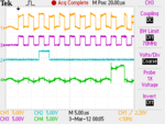
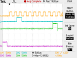
Now, the above scope image was from a standalone 74hc595 that I was testing. I'm now attaching a scope image of the 74hc595 embedded in one of the boards I'm having trouble with. As you can see there's some very clear ringing on the output of the 74hc595 which maybe causes this problem.

In the image there are four signals. The purple line is the shift clock going into the first board. The blue line is the input data line to the first board. The green line is SQh which is output from first board and is supposed to be the input the second board. The Orange line is also the shift clock, but the reason it looks different than the purple line is because I pass it through a buffer on that board so that I can use it as input to the second board without having to worry that the line travels too far. So the orange line is basically the shift clock passed through a buffer.

But it's obvious that the signals coming out of the first board (green and orange) have some series ringing in it which maybe what is causing all this trouble? What typically causes this? There are filtering capacitors (0.1uF and 10uF) between power and gnd at all the chips. And how do I get rid of this ringing.

Thanks,
Matt

F0006TEK.png
 

Status
Not open for further replies.

Part and Inventory Search

Welcome to EDABoard.com

Sponsor

Back
Top