Continue to Site

Welcome to EDAboard.com

Welcome to our site! EDAboard.com is an international Electronics Discussion Forum focused on EDA software, circuits, schematics, books, theory, papers, asic, pld, 8051, DSP, Network, RF, Analog Design, PCB, Service Manuals... and a whole lot more! To participate you need to register. Registration is free. Click here to register now.

5.8GHz RF amplifier custom PCB low power output

Status
Not open for further replies.

susanbod

Newbie level 6
Joined
Jun 16, 2021
Messages
13
Helped
0
Reputation
0
Reaction score
0
Trophy points
1
Activity points
109
Hi everyone :)

I've recently started with RF design. So I tried to amplify a 12dbm output power.

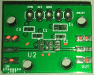
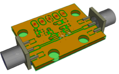
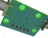
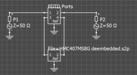
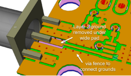
I replicated the HMC407MS8G Evaluation board (https://www.analog.com/media/en/technical-documentation/data-sheets/hmc407.pdf) on a 4 layer PCB

The PCBs were made in JLC PCB using the following stack up my 4 layer board. The trace width was calculated as 0.29 mm for 50 ohm impedance trace.


1623917689773.png


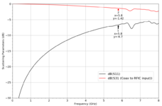
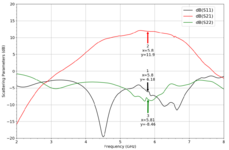
So I finally got the PCB, connected the amplifier to a 12 dBm output power VCO to test the amplification and noticed the amplifier's the output increased only by 1dB. Total output power was 13dBm

Can someone please help? I'm more than happy to share the designs. Every time I try to replicate simple RF boards the power is no where near what its supposed to be 😞

1623918272006.png
 

Your layout shows have very few vias. Do you have enough vias to connect top ground with inner ground layer? The eval PCB shown in the data shows the required placements and amount of vias.

Also, can you show a detail photo of your RF connectors at the PCB? Often there is a gap between conector griund and PCB ground, which introduces series inductance.
 
An important design detail of the original eval board are the vias connecting the exposed pad to the ground plane. Also via fences for the input and output lines.

Original PCB is apparently two layer Rogers, 50 ohm traces are 0.5 mm wide.

1623938708869.png
 
Your layout shows have very few vias. Do you have enough vias to connect top ground with inner ground layer? The eval PCB shown in the data shows the required placements and amount of vias.

Also, can you show a detail photo of your RF connectors at the PCB? Often there is a gap between conector griund and PCB ground, which introduces series inductance.
Hi Volker

Thank you for having a look :)

I agree the vias might have been on the lower end.. but do you think that will reduce its gain to 1dB gain (while it has a gain of 15dB)

The 4 layers are
Layer 1: RF surrounded by Ground
Layer 2: Ground
Layer 3: Power
layer 4: Ground


This is a picture of the SMA connectors, I used these https://uk.rs-online.com/web/p/coaxial-connectors/5265785

1623939062588.png


1623939184660.png
 

An important design detail of the original eval board are the vias connecting the exposed pad to the ground plane. Also via fences for the input and output lines.

Original PCB is apparently two layer Rogers, 50 ohm traces are 0.5 mm wide.

View attachment 170220

Hi FvM,

Thanks for taking time to look at this. You guys are great!

I literally have no one to ask in our institution 😞

I did have ground the exposed pad to the ground plane :). I guess I went easy on the via fences as you mentioned.
The PCB material used is FR4, and I dont have the current funds to purchase Roger boards. Hence I went with the controlled impedance option at JLCPCB.

Thank you
 

I agree the vias might have been on the lower end.. but do you think that will reduce its gain to 1dB gain (while it has a gain of 15dB)

Yes, vias are of extreme importance here. All grounds must be stitched together with small spacing, otherwise the "open end" segements of ground are no longer ground and create unpreditable parasitics.

At the connector, there is no clean transition from SMA ground to effective PCB ground. Just imagine the current path including the (few) vias. At the center pin, I think impedance is much below 50 Ohm: wide pad and small distance to ground.

In addition, there is a gap between coax ground (body) and PCB ground. This will hurt especially at higher frequencies.

I did a quick check of your 50 Ohm line dimensions, that looks ok if vias connect the botoom + side ground properly.
 

Attachments

  • gap_50_200.PNG
    gap_50_200.PNG
    64.3 KB · Views: 120
  • coax7_gaps.PNG
    coax7_gaps.PNG
    83.9 KB · Views: 121
  • coax5_gaps.PNG
    coax5_gaps.PNG
    81.2 KB · Views: 124
  • coax6_gaps.PNG
    coax6_gaps.PNG
    55.4 KB · Views: 119
Last edited:
Yes, vias are of extreme importance here. All grounds must be stitched together with small spacing, otherwise the "open end" segements of ground are no longer ground and create unpreditable parasitics.

At the connector, there is no clean transition from SMA ground to effective PCB ground. Just imagine the current path including the (few) vias. At the center pin, I think impedance is much below 50 Ohm: wide pad and small distance to ground.

In addition, there is a gap between coax ground (body) and PCB ground. This will hurt especially at higher frequencies.

I did a quick check of your 50 Ohm line dimensions, that looks ok if vias connect the botoom + side ground properly.
Hi Volker,

Thanks for that. Really impressed with what you did there.


At the connector, there is no clean transition from SMA ground to effective PCB ground
I thought the PCB top layer ground with a via (or two) would be sufficient. You can see the vias in the below figure (forgot to color those for the amplifiers pad). There's not many of them, but they do connect the ground layers to one another. It's just hard for me to understand that adding more vias in the PCB ground for the SMA ground to connect it to the rest of the ground would push the gain by 14dB higher.


1623948269388.png


At the center pin, I think impedance is much below 50 Ohm: wide pad and small distance to ground.
Is there anything I can do about this? Or verify that this is behind the gain loss?


Again, thank you for your time
 

Attachments

  • 1623948579279.png
    1623948579279.png
    1.6 MB · Views: 112

Additional point, you generally don't want thermals for SMD pads on microwave PCB, although they ease hand soldering and rework. You should rather follow the ground connection style used on the evaluation board, particularly for bypass capacitors, additional amplifier ground pads, connectors. Notice that power supply bypass capacitors have lower distance to amp and wider connection trace on eval board.
 
Your soldering are too bad and VIAs are very few around GND Connection of the Connectors.This IC has a capability to give typical 25dBm Output Power but the board should have been tested with a VNA first at low RF level. Because if there is no protection circuit, transient regime may blow the IC while testing.SMA Connectors re not very appropriate for 5.8GHz so you should use high quality Touching Type ( short inner PIN ) SMA Connectors.
 
There's not many of them, but they do connect the ground layers to one another. It's just hard for me to understand that adding more vias in the PCB ground for the SMA ground to connect it to the rest of the ground would push the gain by 14dB higher.

Yes, I saw those vias, but it's far from what an RF designer would create. You have lots of small issues in many places, and these can add up to a large problem.

Regarding the wide pad, you need to control (reduce) shunt capacitance there. One option might be to keep out the inner ground layer and/or increase spacing to side grounds. I usually use EM simulation to design such transitions.

If you want to upload your Gerber file, I can do a quick EM simulation of your existing layout.
 
Additional point, you generally don't want thermals for SMD pads on microwave PCB, although they ease hand soldering and rework. You should rather follow the ground connection style used on the evaluation board, particularly for bypass capacitors, additional amplifier ground pads, connectors. Notice that power supply bypass capacitors have lower distance to amp and wider connection trace on eval board.
Thank you FvM. I'll take that into account :)

Appreciate your help
 

Your soldering are too bad and VIAs are very few around GND Connection of the Connectors.This IC has a capability to give typical 25dBm Output Power but the board should have been tested with a VNA first at low RF level. Because if there is no protection circuit, transient regime may blow the IC while testing.SMA Connectors re not very appropriate for 5.8GHz so you should use high quality Touching Type ( short inner PIN ) SMA Connectors.
Hi BigBoss

Thank you for taking the time to share your knowledge with me. I'm in the process of learning and I can see I still have a long way to go.

I'll keep this in mind. It's just been a painful experience because I have been trying to replicate analog devices RF amplifiers for so long and they always have less than 25% of their amplification performance.

Thanks for your help :)
 

Yes, I saw those vias, but it's far from what an RF designer would create. You have lots of small issues in many places, and these can add up to a large problem.

Regarding the wide pad, you need to control (reduce) shunt capacitance there. One option might be to keep out the inner ground layer and/or increase spacing to side grounds. I usually use EM simulation to design such transitions.

If you want to upload your Gerber file, I can do a quick EM simulation of your existing layout.
Volker that would be great! Maybe even tell me what tools you use to do it, so I can adopt your method in the future.

I'm trying to get better at RF design. It's just really hard to find the help needed. I appreciate your efforts :)

I have uploaded the Gerber file

Thanks Volker!
 

Attachments

  • HMC407_2021-06-17.zip
    52 KB · Views: 74

Hi Susan,

I simulated your PCB using my 3D EM solver (Empire XPU). Results show issues with the PCB (poor matching from coax to amp) but total gain is not as bad as you reported. There must be some additional issue.

Circuit simulation is linear simulation (small signal) using the manufacturers S-Params for HMC407.

BR, Volker
 

Attachments

  • model_3D.png
    model_3D.png
    182.5 KB · Views: 119
  • model_3D_vias.png
    model_3D_vias.png
    505.8 KB · Views: 131
  • input_path_sparams.png
    input_path_sparams.png
    62.6 KB · Views: 117
  • network_sim.png
    network_sim.png
    30.4 KB · Views: 130
  • network_sparams_with_amp.png
    network_sparams_with_amp.png
    93.5 KB · Views: 158
Hi Susan,

I simulated your PCB using my 3D EM solver (Empire XPU). Results show issues with the PCB (poor matching from coax to amp) but total gain is not as bad as you reported. There must be some additional issue.

Circuit simulation is linear simulation (small signal) using the manufacturers S-Params for HMC407.

BR, Volker
Volker that's amazing work! thank you so much. I'll actually learn how to use that EM solver of yours :)! Looks really professional! Where is the poor matching? and is it something I can resolve in future models Volker ?

I can't think of an additional issue... Could it perhaps be the SMA and pad connection that causes some kind of mismatch ?
1624018307063.png


Thanks Volker you're the best!
 

Yes, as I mentioned earlier (before simulations) the transition to coax looks bad: to wide pad = too much shunt C = too low line imepdance.

I did a quick test with two three modifications to the input section:
- cutout in ground plane under the pad, to reduce excessive shunt capacitance
- added via fence for proper connection of grounds
- added more vias at the ground pads

With that change, matching of the input section is very much improved already.

PS: Looks professional? I hope so, that's the work that I am doing for the last 25 years as an RF simulation specialist ...
 

Attachments

  • s11results_mod.png
    s11results_mod.png
    231.4 KB · Views: 126
  • results_mod.png
    results_mod.png
    74.8 KB · Views: 119
  • layout_mod.png
    layout_mod.png
    250.1 KB · Views: 187

Yes, as I mentioned earlier (before simulations) the transition to coax looks bad: to wide pad = too much shunt C = too low line imepdance.

I did a quick test with two three modifications to the input section:
- cutout in ground plane under the pad, to reduce excessive shunt capacitance
- added via fence for proper connection of grounds
- added more vias at the ground pads

With that change, matching of the input section is very much improved already.

PS: Looks professional? I hope so, that's the work that I am doing for the last 25 years as an RF simulation specialist ...
You Sir are amazing!!
25 years, wow. Beats everyone I know in this profession :)

I really appreciate your help. I can't believe how far you've taken this from the original attempt.
I'll attempt these changes in a newer model and assemble it!

Thanks a million @volker@muehlhaus
 

Yes, as I mentioned earlier (before simulations) the transition to coax looks bad: to wide pad = too much shunt C = too low line imepdance.

I did a quick test with two three modifications to the input section:
- cutout in ground plane under the pad, to reduce excessive shunt capacitance
- added via fence for proper connection of grounds
- added more vias at the ground pads

With that change, matching of the input section is very much improved already.

PS: Looks professional? I hope so, that's the work that I am doing for the last 25 years as an RF simulation specialist ...
Hi Volker :)

Hope you're doing well!

Just wanted to ask you if the cutout in the 2nd ground layer was applied to both SMA pads? Or was it only the first pad ? (even though you mentioned the input section:D )

As for the Gerber file simulation, would CST also be able to get the job done. That's the only EM sim software I've got my hands on at the moment.

Thank you as always :)
 

Yes, the change that I showed for the input path also applies to the output path.

Regarding CST, yes that can also be used. The Empire XPU solver that I used is much faster, but CST can do the job as well.
 
Status
Not open for further replies.

Part and Inventory Search

Welcome to EDABoard.com

Sponsor

Back
Top