Continue to Site

Welcome to EDAboard.com

Welcome to our site! EDAboard.com is an international Electronics Discussion Forum focused on EDA software, circuits, schematics, books, theory, papers, asic, pld, 8051, DSP, Network, RF, Analog Design, PCB, Service Manuals... and a whole lot more! To participate you need to register. Registration is free. Click here to register now.

How to locate a DFlipFlop in a specific SLICE

Status
Not open for further replies.

msdarvishi

Full Member level 4
Joined
Jul 30, 2013
Messages
230
Helped
1
Reputation
2
Reaction score
1
Trophy points
18
Activity points
2,349
Hello friends,

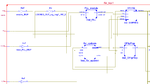
I have a 64-bit LFSR that I've implemented into FPGA and I defined my own UCF in order to control the mapping. AS you see below, the first output of LFSR called cnt_0 is located as:

INST "Inst_lfsr_updown/cnt_0" LOC =SLICE_X0Y0;

now, I have a DFlip-Flop that I would like to put it in the same SLICE (I mean SLICE_X0Y0) in any of 4 available flip-flops in this slice. I checked the BEL constraint on page 72 of this userguide: https://www.xilinx.com/support/documentation/sw_manuals/xilinx11/cgd.pdf

and I defined my constraint for DFlipFlop as the following:

INST "Inst_DFlipFlop" LOC="SLICE_X0Y0" | BEL=FFC;

but in mapping process, I receive the following error that fails the progress:


ERROR:pack:2811 - Directed packing was unable to obey the user design
constraints (LOC=SLICE_X0Y0) which requires the combination of the symbols
listed below to be packed into a single SLICEM component.
The directed pack was not possible because: Two or more symbols belong to
different KEEP_HIERARCHY boundaries and can not be merged into the same
component.
The symbols involved are:
FLOP symbol "Inst_DFlipFlop/Q" (Output Signal = QFlipFlop_OBUF)
FLOP symbol "Inst_lfsr_updown/cnt_0" (Output Signal = DIN<0>)


Anyone can guide me how to tackle this problem?

Thank you all,


Hi,

Can you post your ucf ?


Hello @rahdirs,

Here is my complete UCF that I am trying to locate a DFlipFlop in the flip lop of SLICE_X0Y0.

--------------------------------------------------------------------------

# clock pin for Genesys board
NET "clk_in" LOC = AG18;
NET "clk_in" PERIOD = 10 ns;


# On board push button
NET "reset_lfsr" LOC = AG10;
NET "reset_PLL" LOC = AG11;


# Count_top output pins
NET "count_top[0]" LOC = AA25;
NET "count_top[1]" LOC = AA26;
NET "count_top[2]" LOC = AB27;
NET "count_top[3]" LOC = AC27;
NET "count_top[4]" LOC = Y24;
NET "count_top[5]" LOC = AA24;
NET "count_top[6]" LOC = AB25;
NET "count_top[7]" LOC = AB26;
NET "count_top[8]" LOC = AC28;
NET "count_top[9]" LOC = AD27;
NET "count_top[10]" LOC = AB28;
NET "count_top[11]" LOC = AA28;
NET "count_top[12]" LOC = AG28;
NET "count_top[13]" LOC = AH28;
NET "count_top[14]" LOC = AE28;
NET "count_top[15]" LOC = AF28;
NET "count_top[16]" LOC = AK26;
NET "count_top[17]" LOC = AJ27;
NET "count_top[18]" LOC = AK29;
NET "count_top[19]" LOC = AJ29;
NET "count_top[20]" LOC = AK28;
NET "count_top[21]" LOC = AK27;
NET "count_top[22]" LOC = AH27;
NET "count_top[23]" LOC = AJ26;
NET "count_top[24]" LOC = AJ25;
NET "count_top[25]" LOC = AH25;
NET "count_top[26]" LOC = AF24;
NET "count_top[27]" LOC = AG25;
NET "count_top[28]" LOC = AG27;
NET "count_top[29]" LOC = AG26;
NET "count_top[30]" LOC = AF25;
NET "count_top[31]" LOC = AF26;
NET "count_top[32]" LOC = AE27;
NET "count_top[33]" LOC = AE26;
NET "count_top[34]" LOC = AC25;
NET "count_top[35]" LOC = AC24;
NET "count_top[36]" LOC = AD26;
NET "count_top[37]" LOC = AD25;
NET "count_top[38]" LOC = AD24;
NET "count_top[39]" LOC = AE24;
NET "count_top[40]" LOC = AF13;
NET "count_top[41]" LOC = AG12;
NET "count_top[42]" LOC = AE22;
NET "count_top[43]" LOC = AE23;
NET "count_top[44]" LOC = AE14;
NET "count_top[45]" LOC = AF14;
NET "count_top[46]" LOC = AF20;
NET "count_top[47]" LOC = AF21;
NET "count_top[48]" LOC = AF15;
NET "count_top[49]" LOC = AE16;
NET "count_top[50]" LOC = AE21;
NET "count_top[51]" LOC = AD20;
NET "count_top[52]" LOC = AF16;
NET "count_top[53]" LOC = AE17;
NET "count_top[54]" LOC = AH10;
NET "count_top[55]" LOC = AD19;
NET "count_top[56]" LOC = AG22;
NET "count_top[57]" LOC = AE19;
NET "count_top[58]" LOC = AF23;
NET "count_top[59]" LOC = AE12;
NET "count_top[60]" LOC = AJ10;
NET "count_top[61]" LOC = AF11;
NET "count_top[62]" LOC = AH9;
NET "count_top[63]" LOC = AH8;


# Inputs pins
NET "enable" LOC = AH12;
NET "up_down" LOC = AG8;


# Outputs pins
NET "LOCKED_OUT_PLL" LOC = AG23;
NET "overflow" LOC = AE13;
NET "CLK0_OUT_PLL" LOC = AJ9;
NET "QFlipFlop" LOC = AE11;


INST "Inst_lfsr_updown/cnt_0" LOC =SLICE_X0Y0;
INST "Inst_SIMPREG/DOUT_0" LOC =SLICE_X1Y0;

INST "Inst_lfsr_updown/cnt_1" LOC =SLICE_X2Y0;
INST "Inst_SIMPREG/DOUT_1" LOC =SLICE_X3Y0;

INST "Inst_lfsr_updown/cnt_2" LOC =SLICE_X4Y0;
INST "Inst_SIMPREG/DOUT_2" LOC =SLICE_X5Y0;

INST "Inst_lfsr_updown/cnt_3" LOC =SLICE_X6Y0;
INST "Inst_SIMPREG/DOUT_3" LOC =SLICE_X7Y0;

INST "Inst_lfsr_updown/cnt_4" LOC =SLICE_X8Y0;
INST "Inst_SIMPREG/DOUT_4" LOC =SLICE_X9Y0;

INST "Inst_lfsr_updown/cnt_5" LOC =SLICE_X10Y0;
INST "Inst_SIMPREG/DOUT_5" LOC =SLICE_X11Y0;

INST "Inst_lfsr_updown/cnt_6" LOC =SLICE_X12Y0;
INST "Inst_SIMPREG/DOUT_6" LOC =SLICE_X13Y0;

INST "Inst_lfsr_updown/cnt_7" LOC =SLICE_X14Y0;
INST "Inst_SIMPREG/DOUT_7" LOC =SLICE_X15Y0;

INST "Inst_lfsr_updown/cnt_8" LOC =SLICE_X16Y0;
INST "Inst_SIMPREG/DOUT_8" LOC =SLICE_X17Y0;

INST "Inst_lfsr_updown/cnt_9" LOC =SLICE_X18Y0;
INST "Inst_SIMPREG/DOUT_9" LOC =SLICE_X19Y0;

INST "Inst_lfsr_updown/cnt_10" LOC =SLICE_X20Y0;
INST "Inst_SIMPREG/DOUT_10" LOC =SLICE_X21Y0;

INST "Inst_lfsr_updown/cnt_11" LOC =SLICE_X22Y0;
INST "Inst_SIMPREG/DOUT_11" LOC =SLICE_X23Y0;

INST "Inst_lfsr_updown/cnt_12" LOC =SLICE_X24Y0;
INST "Inst_SIMPREG/DOUT_12" LOC =SLICE_X25Y0;

INST "Inst_lfsr_updown/cnt_13" LOC =SLICE_X26Y0;
INST "Inst_SIMPREG/DOUT_13" LOC =SLICE_X27Y0;

INST "Inst_lfsr_updown/cnt_14" LOC =SLICE_X28Y0;
INST "Inst_SIMPREG/DOUT_14" LOC =SLICE_X29Y0;

INST "Inst_lfsr_updown/cnt_15" LOC =SLICE_X30Y0;
INST "Inst_SIMPREG/DOUT_15" LOC =SLICE_X31Y0;

INST "Inst_lfsr_updown/cnt_16" LOC =SLICE_X32Y0;
INST "Inst_SIMPREG/DOUT_16" LOC =SLICE_X33Y0;

INST "Inst_lfsr_updown/cnt_17" LOC =SLICE_X34Y0;
INST "Inst_SIMPREG/DOUT_17" LOC =SLICE_X35Y0;

INST "Inst_lfsr_updown/cnt_18" LOC =SLICE_X36Y0;
INST "Inst_SIMPREG/DOUT_18" LOC =SLICE_X37Y0;

INST "Inst_lfsr_updown/cnt_19" LOC =SLICE_X38Y0;
INST "Inst_SIMPREG/DOUT_19" LOC =SLICE_X39Y0;

INST "Inst_lfsr_updown/cnt_20" LOC =SLICE_X40Y0;
INST "Inst_SIMPREG/DOUT_20" LOC =SLICE_X41Y0;

INST "Inst_lfsr_updown/cnt_21" LOC =SLICE_X42Y0;
INST "Inst_SIMPREG/DOUT_21" LOC =SLICE_X43Y0;

INST "Inst_lfsr_updown/cnt_22" LOC =SLICE_X44Y0;
INST "Inst_SIMPREG/DOUT_22" LOC =SLICE_X45Y0;

INST "Inst_lfsr_updown/cnt_23" LOC =SLICE_X46Y0;
INST "Inst_SIMPREG/DOUT_23" LOC =SLICE_X47Y0;

INST "Inst_lfsr_updown/cnt_24" LOC =SLICE_X48Y0;
INST "Inst_SIMPREG/DOUT_24" LOC =SLICE_X49Y0;

INST "Inst_lfsr_updown/cnt_25" LOC =SLICE_X50Y0;
INST "Inst_SIMPREG/DOUT_25" LOC =SLICE_X51Y0;

INST "Inst_lfsr_updown/cnt_26" LOC =SLICE_X52Y0;
INST "Inst_SIMPREG/DOUT_26" LOC =SLICE_X53Y0;

INST "Inst_lfsr_updown/cnt_27" LOC =SLICE_X54Y0;
INST "Inst_SIMPREG/DOUT_27" LOC =SLICE_X55Y0;

INST "Inst_lfsr_updown/cnt_28" LOC =SLICE_X56Y0;
INST "Inst_SIMPREG/DOUT_28" LOC =SLICE_X57Y0;

INST "Inst_lfsr_updown/cnt_29" LOC =SLICE_X58Y0;
INST "Inst_SIMPREG/DOUT_29" LOC =SLICE_X59Y0;

INST "Inst_lfsr_updown/cnt_30" LOC =SLICE_X58Y1;
INST "Inst_SIMPREG/DOUT_30" LOC =SLICE_X59Y1;

INST "Inst_lfsr_updown/cnt_31" LOC =SLICE_X56Y1;
INST "Inst_SIMPREG/DOUT_31" LOC =SLICE_X57Y1;

INST "Inst_lfsr_updown/cnt_32" LOC =SLICE_X54Y1;
INST "Inst_SIMPREG/DOUT_32" LOC =SLICE_X55Y1;

INST "Inst_lfsr_updown/cnt_33" LOC =SLICE_X52Y1;
INST "Inst_SIMPREG/DOUT_33" LOC =SLICE_X53Y1;

INST "Inst_lfsr_updown/cnt_34" LOC =SLICE_X50Y1;
INST "Inst_SIMPREG/DOUT_34" LOC =SLICE_X51Y1;

INST "Inst_lfsr_updown/cnt_35" LOC =SLICE_X48Y1;
INST "Inst_SIMPREG/DOUT_35" LOC =SLICE_X49Y1;

INST "Inst_lfsr_updown/cnt_36" LOC =SLICE_X46Y1;
INST "Inst_SIMPREG/DOUT_36" LOC =SLICE_X47Y1;

INST "Inst_lfsr_updown/cnt_37" LOC =SLICE_X44Y1;
INST "Inst_SIMPREG/DOUT_37" LOC =SLICE_X45Y1;

INST "Inst_lfsr_updown/cnt_38" LOC =SLICE_X42Y1;
INST "Inst_SIMPREG/DOUT_38" LOC =SLICE_X43Y1;

INST "Inst_lfsr_updown/cnt_39" LOC =SLICE_X40Y1;
INST "Inst_SIMPREG/DOUT_39" LOC =SLICE_X41Y1;

INST "Inst_lfsr_updown/cnt_40" LOC =SLICE_X38Y1;
INST "Inst_SIMPREG/DOUT_40" LOC =SLICE_X39Y1;

INST "Inst_lfsr_updown/cnt_41" LOC =SLICE_X36Y1;
INST "Inst_SIMPREG/DOUT_41" LOC =SLICE_X37Y1;

INST "Inst_lfsr_updown/cnt_42" LOC =SLICE_X34Y1;
INST "Inst_SIMPREG/DOUT_42" LOC =SLICE_X35Y1;

INST "Inst_lfsr_updown/cnt_43" LOC =SLICE_X32Y1;
INST "Inst_SIMPREG/DOUT_43" LOC =SLICE_X33Y1;

INST "Inst_lfsr_updown/cnt_44" LOC =SLICE_X30Y1;
INST "Inst_SIMPREG/DOUT_44" LOC =SLICE_X31Y1;

INST "Inst_lfsr_updown/cnt_45" LOC =SLICE_X28Y1;
INST "Inst_SIMPREG/DOUT_45" LOC =SLICE_X29Y1;

INST "Inst_lfsr_updown/cnt_46" LOC =SLICE_X26Y1;
INST "Inst_SIMPREG/DOUT_46" LOC =SLICE_X27Y1;

INST "Inst_lfsr_updown/cnt_47" LOC =SLICE_X24Y1;
INST "Inst_SIMPREG/DOUT_47" LOC =SLICE_X25Y1;

INST "Inst_lfsr_updown/cnt_48" LOC =SLICE_X22Y1;
INST "Inst_SIMPREG/DOUT_48" LOC =SLICE_X23Y1;

INST "Inst_lfsr_updown/cnt_49" LOC =SLICE_X20Y1;
INST "Inst_SIMPREG/DOUT_49" LOC =SLICE_X21Y1;

INST "Inst_lfsr_updown/cnt_50" LOC =SLICE_X18Y1;
INST "Inst_SIMPREG/DOUT_50" LOC =SLICE_X19Y1;

INST "Inst_lfsr_updown/cnt_51" LOC =SLICE_X16Y1;
INST "Inst_SIMPREG/DOUT_51" LOC =SLICE_X17Y1;

INST "Inst_lfsr_updown/cnt_52" LOC =SLICE_X14Y1;
INST "Inst_SIMPREG/DOUT_52" LOC =SLICE_X15Y1;

INST "Inst_lfsr_updown/cnt_53" LOC =SLICE_X12Y1;
INST "Inst_SIMPREG/DOUT_53" LOC =SLICE_X13Y1;

INST "Inst_lfsr_updown/cnt_54" LOC =SLICE_X10Y1;
INST "Inst_SIMPREG/DOUT_54" LOC =SLICE_X11Y1;

INST "Inst_lfsr_updown/cnt_55" LOC =SLICE_X8Y1;
INST "Inst_SIMPREG/DOUT_55" LOC =SLICE_X9Y1;

INST "Inst_lfsr_updown/cnt_56" LOC =SLICE_X6Y1;
INST "Inst_SIMPREG/DOUT_56" LOC =SLICE_X7Y1;

INST "Inst_lfsr_updown/cnt_57" LOC =SLICE_X4Y1;
INST "Inst_SIMPREG/DOUT_57" LOC =SLICE_X5Y1;

INST "Inst_lfsr_updown/cnt_58" LOC =SLICE_X2Y1;
INST "Inst_SIMPREG/DOUT_58" LOC =SLICE_X3Y1;

INST "Inst_lfsr_updown/cnt_59" LOC =SLICE_X0Y1;
INST "Inst_SIMPREG/DOUT_59" LOC =SLICE_X1Y1;

INST "Inst_lfsr_updown/cnt_60" LOC =SLICE_X0Y2;
INST "Inst_SIMPREG/DOUT_60" LOC =SLICE_X1Y2;

INST "Inst_lfsr_updown/cnt_61" LOC =SLICE_X2Y2;
INST "Inst_SIMPREG/DOUT_61" LOC =SLICE_X3Y2;

INST "Inst_lfsr_updown/cnt_62" LOC =SLICE_X4Y2;
INST "Inst_SIMPREG/DOUT_62" LOC =SLICE_X5Y2;

INST "Inst_lfsr_updown/cnt_63" LOC =SLICE_X6Y2;
INST "Inst_SIMPREG/DOUT_63" LOC =SLICE_X7Y2;


# AREA_GROUP constraints for instances inside the lfsr_top module
INST "Inst_PLL" AREA_GROUP = "pblock_Inst_PLL";

AREA_GROUP "pblock_Inst_PLL" RANGE=SLICE_X2Y6:SLICE_X5Y9;


## Locating DFlipFlop in an arbitrary place...
INST "Inst_DFlipFlop" LOC=SLICE_X0Y0 | BEL=FFC;


INST "Inst_SIMPREG" AREA_GROUP = "pblock_Inst_SIMPREG";

INST "LOCKED_OUT_sig_neg1_INV_0" LOC = SLICE_X27Y4;
 

INST "Inst_lfsr_updown/cnt_0" LOC =SLICE_X0Y0;

INST "Inst_DFlipFlop" LOC="SLICE_X0Y0" | BEL=FFC;

Two or more symbols belong to different KEEP_HIERARCHY boundaries and can not be merged into the same
component.
Seems it tells you what is wrong. You have them in different hierarchical boundaries, try turning off keep hierarchy in the XST synthesis options and flatten the design, and/or try rebuilt.

see these two links on similar issues.
http://forums.xilinx.com/t5/Synthesis/Keeping-Hierarchy-causes-packing-error-with-PicoBlaze-6/td-p/122850
http://www.xilinx.com/support/answers/30705.html


Hello @ads-ee,

Thanks for your reply. I did turning off the Hierarchy and also Rebuilt but I still have the same error. Neither those links couldn't solve the problem since they concern about LUTs. The current error is:


ERROR:pack:2811 - Directed packing was unable to obey the user design
constraints (LOC=SLICE_X1Y0) which requires the combination of the symbols
listed below to be packed into a single SLICEL component.

The directed pack was not possible because: The clock enable signals don't
agree.
The symbols involved are:
FLOP symbol "Inst_DFlipFlop/Q" (Output Signal = Q)
FLOP symbol "Inst_SIMPREG/DOUT_0" (Output Signal = DOUT_0)
 

ERROR:pack:2811 - Directed packing was unable to obey the user design
constraints (LOC=SLICE_X1Y0) which requires the combination of the symbols
listed below to be packed into a single SLICEL component.

The directed pack was not possible because: The clock enable signals don't
agree.

The symbols involved are:
FLOP symbol "Inst_DFlipFlop/Q" (Output Signal = Q)
FLOP symbol "Inst_SIMPREG/DOUT_0" (Output Signal = DOUT_0)

The control sets have to be identical to pack registers into the same slice. I think you should go back and re-read the documentation on the logic blocks paying particular attention to the details of what is supported.

I originally assumed you knew about the control set restrictions, besides your original post didn't mention anything about the clock enable.

Actually come to think of it, the previous problem with the hierarchy was probably masking this problem.


Hello again,

in order to synchronize the control sets, I defined a CE (clock enable) pin for my DFlipFlop and I connected it to the global enable of my top module, the same enable as whole circuit. Bu still have the Error 2811, but with different message, this time.

Really I do not know what to do to overcome this problem...??!!! :(
 

Really I do not know what to do to overcome this problem...??!!! :(
I'm guessing that it's likely you're trying to solve the wrong problem. Here are some questions for you to ponder:
- What problem(s) do you think you're solving by trying to place things in particular locations?
- Have you tried removing all of the placement constraints (except top level pin locations, if the board pinout has already been defined). When you do that, does the design meet all performance requirements (i.e. Fmax, Tsu, Tco, Tpd)?. If so, then why are you trying to define particular locations?

Kevin Jennings
 

As Kevin says, why are you doing this? There is a reason Xilinx created the program MAP.exe and the program PAR.exe so you don't have to do the mapping of logic yourself. Perhaps you think you can do a better job than Xilinx does?

If you insist on continuing with this, you'll have to keep fixing each problem as the come up until you've got the correct control sets and the logic can reside in the same slice. Personally I think you're just wasting your time.
 

[URGENT] How to solve Mapping problem ERROR:Pack:2811

Hello friends,

I have a design comprised of a PLL, an LFSR, a Register (called SIMPREG schematic) and a DFlipFlop. I am trying to locate the DflipFlop in the same slice of one signal of LFSR (called cnt_0). The schematic of the synthesized design is shown below. While I am trying to implement it, I see the mapping error showing the disagree of clock enable or clock signal. I did lotfs of trials but I do not know how to solve this problem. Can anybody help me with that?
I also posted my DflipFlop code and my LFSR showing that both of them have synchronous clocks. Sometimes I was receiving the error mentioning that "a flop using a synchronous clock cannot be located in a place that has async clock signal, so I tried to solve this part but the whole problem still remained).


DFlipFlop VHDL code:
------------------------------

entity DFlipFlop is
Port ( D : in STD_LOGIC;
CLK_D : in STD_LOGIC;
CE : in STD_LOGIC;
reset : in STD_LOGIC;
Q : out STD_LOGIC);
end DFlipFlop;

architecture Behavioral of DFlipFlop is
begin
process(CLK_D)--,reset)

begin
if (rising_edge(CLK_D)) then
if (reset = '0') then -- added
Q <= D;
else
Q <= '0';
end if;
end if;
end process;
end Behavioral;


my UCF part that merges 2 components in SLICE_X0Y0
--------------------------------------------------------------------------

INST "Inst_lfsr_updown/cnt_0" LOC =SLICE_X0Y0;

INST "Inst_DFlipFlop" LOC=SLICE_X0Y0;


ERROR:pack:2811 - Directed packing was unable to obey the user design
constraints (LOC=SLICE_X0Y0) which requires the combination of the symbols
listed below to be packed into a single SLICEM component.
The directed pack was not possible because: The clock enable signals don't
agree.
The symbols involved are:
FLOP symbol "Inst_DFlipFlop/Q" (Output Signal = Q)
FLOP symbol "Inst_lfsr_updown/cnt_0" (Output Signal = DIN<0>)
Mapping completed.


Thank you all,


This is the synthesized schematic of the design...
 

Attachments

  • Screenshot8.png
    Screenshot8.png
    48.7 KB · Views: 59
Last edited by a moderator:

Re: [URGENT] How to solve Mapping problem ERROR:Pack:2811

Hi,

This is same as your post the other day :
D-Flip flop Slice#post1436164
Why are you trying to push DflipFlop into the same slice of one signal of LFSR ?
 

Go re-read my response in post #8.

Control sets are comprised of: clock, enable, and reset or set. All of these signals have to be driven by identical sources if you want the FFs to be in the same slice. If you are not using a enable on one FF then it can't be placed in the same slice as a FF that uses an enable. Or in your case you are using the enable as a reset in another FF.

It's pretty obvious from the schematic that you are not making sure the FFs all have identical control sets and have not changed that approach since I told you the control sets had to be identical.
 

Addendum:

You can force the tools to not use any of the Slice control pins like clock enables and resets (asynchronous/synchornous) and force both clock enables and resets (synchronous only) into the LUT logic. In ISE this should be under the Xilinx Specific Options of XST process properties: -use_clock_enable, -use_sync_set, -use_sync_reset should all be set to NO to force the equivalent logic to be implemented in LUTs.
 

Status
Not open for further replies.

Part and Inventory Search

Welcome to EDABoard.com

Sponsor

Back
Top