Continue to Site

Welcome to EDAboard.com

Welcome to our site! EDAboard.com is an international Electronics Discussion Forum focused on EDA software, circuits, schematics, books, theory, papers, asic, pld, 8051, DSP, Network, RF, Analog Design, PCB, Service Manuals... and a whole lot more! To participate you need to register. Registration is free. Click here to register now.

[SOLVED] Diode Clamped Converter

Status
Not open for further replies.

danilorj

Member level 3
Joined
Apr 17, 2014
Messages
60
Helped
1
Reputation
2
Reaction score
1
Trophy points
8
Activity points
462
Hi guys,
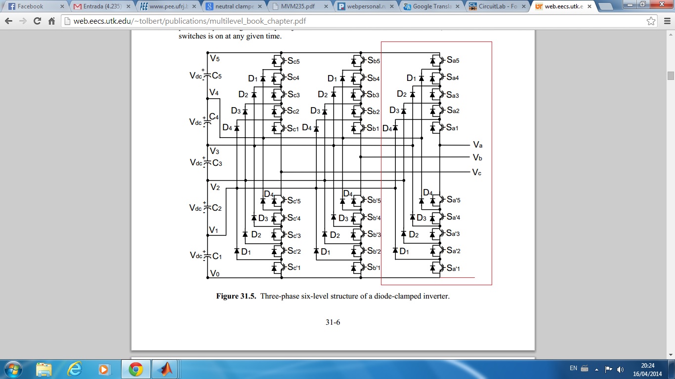
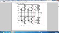
I'm trying to analyse the principle of working of this diode clamped multilevel inverter.
Let's say I want to analyse just the part within the red rectangle in the figure attached.
If all the switches below are on than Va=0, Ok.
Now when Sa1,Sa'5,Sa'4,Sa'3a and Sa'2 are on and Sa'1 is off, Va=Vdc.
This is what I don't understand, I don't understand how these diodes can clampe.
For example, at anode of diode D4 would be Vdc and at the cathode of it what would be?
For it to conduct the cathode voltage should be lower than the anode, how can I assure this?
 

I am running a simulation of a 5-level inverter (single phase), found in this article:


I see only two diodes which are involved in delivering power to the load.


The other diodes conduct for an instant. Yet they are essential toward maintaining a correct waveform. They conduct at certain times, when a combination of switches discharges a capacitor briefly. The diodes may have a function of keeping the capacitor charges balanced.

This circuit puts capacitors in series, charging them from a DC supply. Often this is a dubious design, because the capacitors are likely to acquire mismatching charges.

The circuit can work, but only if the clock signals match very closely.

My simulation is done with Falstad's animated interactive simulator.
This link will open the site falstad.com/circuit, load my schematic into his simulator, and run it on your computer.

https://tinyurl.com/meozuvn

You can watch current bundles travelling through wires, the switches open and close, the scope traces move across the screen, etc.

You can change values at will. Right-click on a component, and select Edit.

Pressing other keys will let you do other things, such as move components, or the entire circuit, etc.
 

This is pretty interesting, I can see the path the current can go through. But I still have one doubt:

Let's say the path the current flows when S1,S2,S3, S8 are off and S4,S5,S6,S7 are on. When the current flows from Switch 7 back to C3 e C4 there is a diode in this path (D1) and three more diodes above of it (D2,D3,D4). Why of if? Only one would not be necessary?


There is another thing I'd like to ask. When the switches S5 to S8 are all set to on and S1 to S4 are all set to off, for example. There is still current running through the upper part of the circuit. It sounds weird. There is no closed path so this current can go through.
 

there is a diode in this path (D1) and three more diodes above of it (D2,D3,D4). Why of if? Only one would not be necessary?

The drop created by 3 diodes may be needed to match the effect of 2+1 diodes elsewhere in the circuit.

In my simulation the diodes rarely conduct. It creates a coarse sinewave. The clock signals are simple and relatively slow.

However the articles speak of applying rapid switching PWM, to create a smooth sinewave. I imagine the diodes come into action for that purpose, as the 'clamping' function.

Or perhaps if the load were to draw unequal current during the positive versus the negative cycle. This would result in unequal charges on the capacitors, unless some safeguard is added.

A simplified version of this topology is the half-bridge. It produces a rectangular waveform. This could be called a 3-level AC inverter.


However the article shows a more elaborate 3-level inverter. It adds 2 switches and the diodes. Yet its output is unchanged from the circuit above.

The additional components would provide no benefit, except that I think the authors must apply rapid PWM, in order to get a more sine-like output.


- - - Updated - - -

There is another thing I'd like to ask. When the switches S5 to S8 are all set to on and S1 to S4 are all set to off, for example. There is still current running through the upper part of the circuit. It sounds weird. There is no closed path so this current can go through.

You are seeing a programming glitch in the simulator. I reduced the 'Off' resistance of the switches. I thought it would help balance the charges on the capacitors. But somehow the switches generate current on their own.

The default value of the switches is 10G when Off. Miniscule current flows then.
 

Status
Not open for further replies.

Similar threads

Part and Inventory Search

Welcome to EDABoard.com

Sponsor

Back
Top