Welcome to our site! EDAboard.com is an international Electronics Discussion Forum focused on EDA software, circuits, schematics, books, theory, papers, asic, pld, 8051, DSP, Network, RF, Analog Design, PCB, Service Manuals... and a whole lot more! To participate you need to register. Registration is free. Click here to register now.
i study a schemic,maybe one gate is enough,it use 3 not gate to drive a digital attenuator,why? for delay or for Amplifier or for enhance driver ability
ya , for delaying purpose they were added the three NOT gate's , its becoming the timing diagram basis . the output inverted value is delayed for some seconds , thats why i think added the extra two NOT gate,.
In normal situations, only one inverter is needed.
But when there are 3 in a row:
* Sometimes the designer adds more gates in order to use up spare gates on an IC.
* Sometimes the initial signal rises or falls slowly. Although one gate supposedly will have a clean output that transitions quickly, the designer might add another gate just in case. Then he must add a third NOT gate to invert the signal back to its polarity as it was after the first NOT gate.
* Sometimes a designer needs just a tiny delay in the signal. Each gate contains numerous transistors. The propagation delays add up to a tiny amount.
* The schematic does not show additional connections, but it would be easy to tap in between the gates to obtain a second signal. Example, an out-of-phase clock signal.
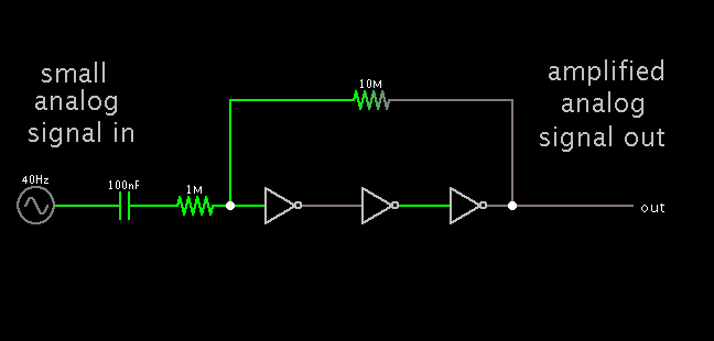
* You mention an amplifier. There is a way to use digital gates in an analog application. 3 inverters and 2 resistors form an amplifier. It doesn't work in the simulator, but it works with real components. The 4069 inverter IC is particularly recommended for this.
In normal situations, only one inverter is needed.
But when there are 3 in a row:
* Sometimes the designer adds more gates in order to use up spare gates on an IC.
* Sometimes the initial signal rises or falls slowly. Although one gate supposedly will have a clean output that transitions quickly, the designer might add another gate just in case. Then he must add a third NOT gate to invert the signal back to its polarity as it was after the first NOT gate.
* Sometimes a designer needs just a tiny delay in the signal. Each gate contains numerous transistors. The propagation delays add up to a tiny amount.
* The schematic does not show additional connections, but it would be easy to tap in between the gates to obtain a second signal. Example, an out-of-phase clock signal.
* You mention an amplifier. There is a way to use digital gates in an analog application. 3 inverters and 2 resistors form an amplifier. It doesn't work in the simulator, but it works with real components. The 4069 inverter IC is particularly recommended for this.
thank you for your detailed help,here is my understand of your answer ,i dont know whether my understand is right
*1 means there maybe some not gates(maybe just 2) we dont use on an ic ,so use 2 unused gates connect with 1 gate,there is no really improvement
*2 i dont understand well,plz explain what in case for ,thx
*3 for delay ,i can understand
*4 means we can get an Additional out-of-phase signal
thank you sir
I guess this is the point you asked me to clarify:
* Sometimes the initial signal rises or falls slowly. Although one gate supposedly will have a clean output that transitions quickly, the designer might add another gate just in case. Then he must add a third NOT gate to invert the signal back to its polarity as it was after the first NOT gate.
Theoretically a logic gate is supposed to output a squarish waveform. It is supposed to clean up a noisy or wandering or ramp shaped input signal.
Its internal network switches most efficiently when the input signal is squarish.
However when the input signal is noisy or wandering or ramp shaped, the internal network spends that much more time in linear (resistive) mode rather than switching mode. The supply may dip a little as a result of additional power being wasted. Etc. (This might happen more with old-fashioned TTL chips which ran on greater current and generated larger spikes on the supply, but my knowledge is incomplete.)
Anyway the result may be a less square waveform than is desired.
So the designer adds a second gate to clean up the waveform a bit more.
He could use a non-inverting buffer. Or he might simply use 2 inverters.
This site uses cookies to help personalise content, tailor your experience and to keep you logged in if you register.
By continuing to use this site, you are consenting to our use of cookies.

")