dumindu89
Member level 1
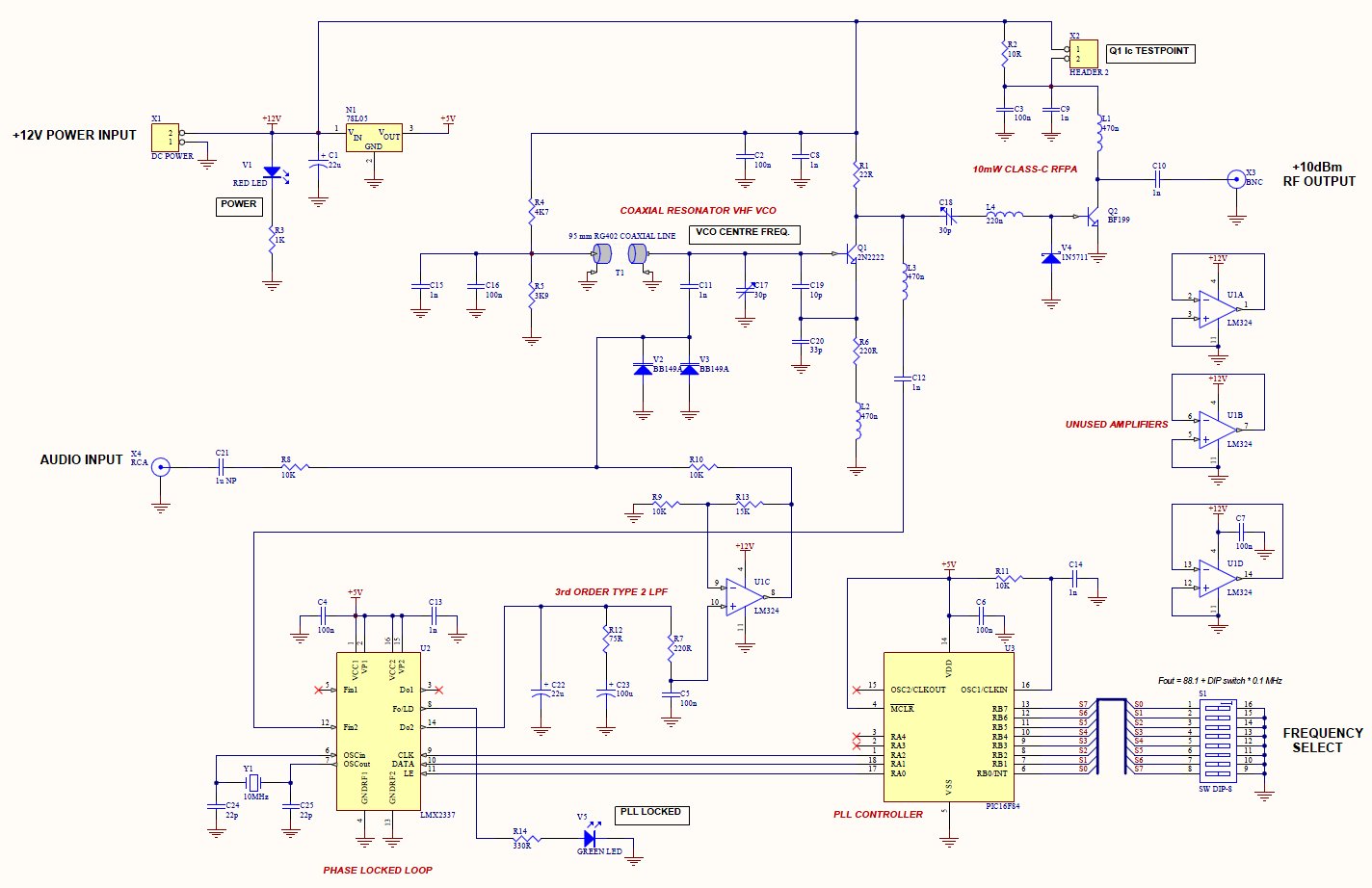
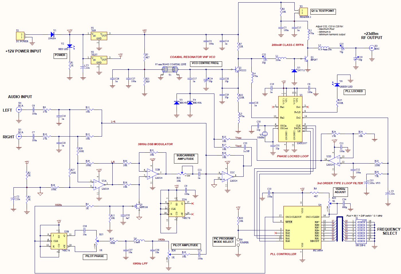
I am going to design a FM modulator based on digital phase locked loop as my final year project. Mainly the FM modulator. The modulator should be programmable to generate FM carrier frequencies in 100 kHz steps. Transmission frequency range: 88MHz - 108 MHz. There should not be interferences between each channel.
Here is the basic block diagram
**broken link removed**
Here I am going to use 74HC4046A IC for the digital phase locked loop and 74HC4059 IC for the programmable divided by N counter. Since the 74HC4046A Ic not working in the FM broadcasting band, a bandpass filter will be used to filter out the desired frequency range from the produced harmonics at the VCO.
I have few questions.
- What are the benefits/advantages of using digital phase locked loop for FM modulation?
- Is it possible to use the 74HC4046A IC for the design? What things should I consider?
- How do I make the 74HC4059 IC as programmable to select the desired chaneel?
- What are the other yhings I should concentrate when I designing this?
Last edited:
")