Continue to Site

Welcome to EDAboard.com

Welcome to our site! EDAboard.com is an international Electronics Discussion Forum focused on EDA software, circuits, schematics, books, theory, papers, asic, pld, 8051, DSP, Network, RF, Analog Design, PCB, Service Manuals... and a whole lot more! To participate you need to register. Registration is free. Click here to register now.

[SOLVED] 1ma constant current source for PT100 sensor (Circuit problem

Status
Not open for further replies.

Ranbeer Singh

Full Member level 5
Joined
Jul 30, 2015
Messages
259
Helped
22
Reputation
44
Reaction score
22
Trophy points
1,298
Location
Faridabad India
Activity points
3,266
Hello

I am making 1ma current source for constant

- - - Updated - - -

Sorry for mistake

Continue......I am making 1ma constant current source for PT100 sensor using OP07 op-amp. I am using a voltage divider for negative pin and a series resistance for positive input pins. At the negative input pin i am generating 4.57V and same on positive pin by a 501E resistance it will drop approximately 0.5V. Same volt at both inputs... and transistor should be generate 1ma constant current.
It's not working according my calculation. When i connect 100E resistance it makes 115mv.

V=I*R
0.001*100 = 0.1v

But it's generating 0.115v. Please help...circuit is given below.

Circuit

https://obrazki.elektroda.pl/9844962300_1455512660.png
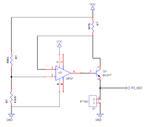
 

Collector current may be 1mA but the emitter current will be 1mA plus the base current, whatever that happens to be.

Replace the bipolar transistor with a Jfet.
The source current will then be exactly the same as drain current, because there is always zero gate current.
 

You are right but i am worry with extra voltage.

- - - Updated - - -

I have decided to use JFET for my circuit. What will be suitable JFET for my application.
 

Use the multimeter and measure exact values of the resistors and calculate the current by hand and the transistor specs.
 

Hi,

I assume VCC is 5V. But OP07 is not specified to operate at 5V.
Additionally there may be an issue wit opamp common mode input voltage range.
Additionally consider a capacitive feedback from opamp output to inverting input and an additional feedback resistor to avoid oscillation.

--> Look for a suitable Opamp. RR input, RR output, unity gain stable.
And as suggested a fet instead of the bjt.

According your voltage reading your supply voltage is slightely higher than 5.00V. Your current is proportional to VCC, so a higher VCC causes higher current. Use a zener or a voltage_reference to improve in this.

Klaus
 

Hi Klaus

Datasheet says Wide input voltage range: ±14 V typical, Wide supply voltage range: ±3 V to ±18 V but you says...

I assume VCC is 5V. But OP07 is not specified to operate at 5V.
 

Hi,

Supply: +/-3 V gives a total of 6V minimal, but you use 5V only.

Input voltage range depends on supply voltage. The given input voltage range is for a supply voltage of +/-15V.
(So about 1V from supply voltage)

Sadly in my (Analog devices) datashheet there is only "input voltage range" specified.
This usually is the differential input voltage range. (With your circuit about 0V)

Good datasheets show:
* differential input voltage range, and
* common mode input voltage range (with your circuit about VCC - 0.5V)

Klaus
 
Thinking about it a bit more, a small n channel mosfet such as a 2N7000 might be better, as it would go straight into your existing circuit without making any other changes.

https://www.fairchildsemi.com/datasheets/2N/2N7000.pdf

Gate threshold for 1mA is 2v typical.
That would fit in quite well with your op amp and +5v supply.
 

Oh

I did not think of it. I have tested my all resistance values by a high quality multimeter. The exact valve was given in my circuit but my theory and practical was not matching to each other.
I will check it with 12v supply.

I am using a 0.1uf capacitor on transistor output...Is is write or wrong?

- - - Updated - - -

what type of BJET will be suitable for it?

- - - Updated - - -

JFET

N-channel or P-channel?
 

The 2N7000 is a small plastic N channel mosfet, and I gave a link to the data sheet.

I never thought to look at the op amp. Duh !

If you have +12v available, that would be much better.
 
Can you please explain why you are sending the feedback into the non-inverting input? How it is going to work in this case?
 

Can you please explain why you are sending the feedback into the non-inverting input? How it is going to work in this case?
The circuit layout is correct.

If current tries to increase, the voltage drop across the 510 ohm resistor increases.
This causes the voltage on pin 3 (non inverting) to fall.
Op amp output falls, current through NPN falls.
So overall feedback is negative.
 
I am permanently confused between NPN and PNP! Thanks for the explanation.
 

I presume you are referring to the circuit linked in post #1

9844962300_1455512660.png

I would suggest some modifications. If no FET is available, you should at least use a Darlington (e.g. BC517 for the NPN configuration) to keep the base current error negligible.

Secondly, the output transistor involves a voltage gain for Rsens < 500 ohm which can make the OP loop unstable, because it's not compensated for feedback factors > 1. The problem can be overcome by using a PNP transistor (or PFET) and an inverting OP configuration, otherwise compensation (e.g. a capacitor from OP output to inverting input) is required.

- - - Updated - - -

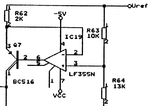
Below an implementation from a real instrument. Vref should be also used for the ADC to make a ratiometric measurement.

1mA.gif
 
Hi,

Can you please explain why you are sending the feedback into the non-inverting input? How it is going to work in this case?
My mistake. I had another circuit in mind with the resisor on the low side.

But a capacitor from output to inverting input is correct...it will stabilize the whole circuit.

Klaus
 

I also have another comment: it is not a good practice to run a complete circuit with a reference voltage because there may be unwanted loading on the Vref. There are reliable and cost-effective solutions for a voltage reference and they should have been used at the appropriate stage rather than using the power supply voltage.
 

I also have another comment: it is not a good practice to run a complete circuit with a reference voltage because there may be unwanted loading on the Vref. There are reliable and cost-effective solutions for a voltage reference and they should have been used at the appropriate stage rather than using the power supply voltage.
Generally correct, but the presented circuit depends at on Vref sourcing the 1 mA current. Using the (analog) power supply as reference can be reasonable if a ratiometric measurement is implemented
 

Using the (analog) power supply as reference can be reasonable if a ratiometric measurement is implemented

If the VCC changes by 20% (say) then the current will also change in a similar manner. This current is being used to measure the resistance of a Pt-resistance thermometer by converting the resistance to a voltage. That purpose will be defeated.
 

We are expecting a regulated analog supply, e.g. +/- 5% tolerance, +/-1 % temperature drift. By using ratiometric measurement (same reference for current source and ADC), the error can be completely eliminated.
 

Status
Not open for further replies.

Similar threads

Part and Inventory Search

Welcome to EDABoard.com

Sponsor

Back
Top