Continue to Site

Welcome to EDAboard.com

Welcome to our site! EDAboard.com is an international Electronics Discussion Forum focused on EDA software, circuits, schematics, books, theory, papers, asic, pld, 8051, DSP, Network, RF, Analog Design, PCB, Service Manuals... and a whole lot more! To participate you need to register. Registration is free. Click here to register now.

1-D Eigenmode Simulation on CST: Dispersion Diagram for a Unit Cell of a Leaky Wave Antenna

Status
Not open for further replies.

KeysorSoze

Newbie level 4
Joined
Mar 6, 2018
Messages
7
Helped
0
Reputation
0
Reaction score
0
Trophy points
1
Activity points
142
Hi,
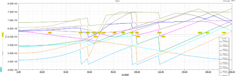
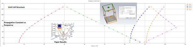
I am trying to perform eigenmode simulation to obtain dispersion diagram for a paper "https://ieeexplore.ieee.org/stamp/stamp.jsp?tp=&arnumber=9055410" Figure 3 (b), but I am not getting the desired result. I have tried performing the simulations in both HFSS and CST and the summary ppt (of errors) along with simulation models (.zip) is attached.

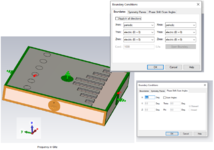
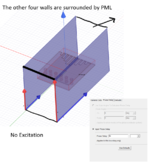
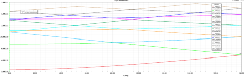
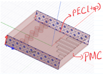
In CST, I have applied periodic boundary condition (with parametric sweep of phase angle difference between the periodic boundaries) in the direction of the guiding structure and the other two boundaries as Electric, but as it turns out the eigenmode are obtained for a waveguide created due to via-walls and electric boundary condition I give (explained in PPT). Hence dispersion diagram is similar to a waveguide. Essentially, I want to figure out the boundary conditions.

I have also attached the simulation model in HFSS in case that is required.

Any help or ideas will be appreciated :)
 

Attachments

  • Capture.PNG
    Capture.PNG
    143.4 KB · Views: 332
  • Capture1.PNG
    Capture1.PNG
    406.9 KB · Views: 364
  • EigenmodeSimulations.zip
    1.6 MB · Views: 263

Solution
Hello all,
Sorry to reply a bit late. But here is my long due resolution .

The key here lies in visualizing each of the mode at different k0*p (or angles). If you look at my graphs that I have attached in my replies, there actually exists the dispersion behaviour of the unit cell that I want to observe. I have highlited the mode, I am looking for in the image attached. Compare it with the one previously posted in the thread.

However, the problem occurs when the simulation softwares mixes the modes. The softwares (SW) here (CST and HFSS) are both sort of dumb. Both the SWs connect the the points (for the modes) which are at the minimum frequency.

To elaborate, if you look at the whole simulation domain it is sort of a waveguide on...
It looks like in your CST, you'd want the boundary on the right to be a PMC rather than a PEC. As you indicated, a PEC isn't quite correct.

In the HFSS simulation, surrounding 4 walls with a PML is probably excessive and may give errors due to the structure being too open. I would at least be sure to simulate a large number of modes and sort through them all for one that looks right (perhaps > 20 modes).
Hello,
Thank you for the reply and pointing out the PMC boundary. I tried simulating with the following boundary conditions (in the screenshot), in both CST and HFSS in eigenmode and got similar results but not of the paper. I simulated until the 20th mode, screenshot attached but none of them seem to match the behavior in the paper.

Also, if possible could you please point out the proper simulation setup values for HFSS for Eigenmode simulation? (I have attached the screenshot (Capture2_Conditions).

In the HFSS simulation, surrounding 4 walls with a PML is probably excessive and may give errors due to the structure being too open.
What should be the optimum distance? I used the classic condition (lamda/4).
 

Attachments

  • Capture_2_S11.PNG
    Capture_2_S11.PNG
    103.1 KB · Views: 264
  • Capture_2.PNG
    Capture_2.PNG
    738.5 KB · Views: 274
  • Capture_2_Conditions.png
    Capture_2_Conditions.png
    146.2 KB · Views: 250

I would like to start this reply by stating that there is no good way to simulate an open domain in HFSS's eigenmode solver -- specifically since it is primarily meant for use with closed structures. That being said, there are many tools that give reasonable results with an open domain, such as PMLs.

Unfortunately, it appears something was horrendously wrong with your setup. Your domain surrounding the unit cell was made of PML material, not air or vacuum. There seemed to be too many PML objects. I deleted all the PMLs and placed impedance boundaries on the outer edges (I've found this to be a reasonable approach, but don't take the resulting data to be 'correct').

This seemed to produce something like the mode you are looking for. I plotted the fifth mode of the simulation (at k_x = 0 degrees) below, which seems to agree with the lower band of the mode you are looking for. See my updated simulation file attached.

Good luck!

1642179554186.png
 

Attachments

  • SarkarPaper_UnitCellSinusoidal.zip
    60.6 KB · Views: 214

I would like to start this reply by stating that there is no good way to simulate an open domain in HFSS's eigenmode solver -- specifically since it is primarily meant for use with closed structures. That being said, there are many tools that give reasonable results with an open domain, such as PMLs.

Unfortunately, it appears something was horrendously wrong with your setup. Your domain surrounding the unit cell was made of PML material, not air or vacuum. There seemed to be too many PML objects. I deleted all the PMLs and placed impedance boundaries on the outer edges (I've found this to be a reasonable approach, but don't take the resulting data to be 'correct').

This seemed to produce something like the mode you are looking for. I plotted the fifth mode of the simulation (at k_x = 0 degrees) below, which seems to agree with the lower band of the mode you are looking for. See my updated simulation file attached.

Good luck!

View attachment 173885
Hey thank you so much for the replies and taking the time for providing help :). But I don't seem to be getting the results. I simulated the model you sent and tried the parametric analysis; I got this (screenshot attached). I think HFSS is finding modes which actually do not exist (or cancel out each other).

I tried the same model with different configurations on CST as well seems like the software is giving the same results for a simple waveguide (without any pattern) and the unit cell.
 

Attachments

  • EDA_Q.PNG
    EDA_Q.PNG
    141.9 KB · Views: 242
  • EDA1_CST.png
    EDA1_CST.png
    162.4 KB · Views: 251
  • EDA2_CST.png
    EDA2_CST.png
    66.5 KB · Views: 234

Great, the CST results look good.

Unfortunately, the PMLs in HFSS are notorious for introducing a host of spurious modes, which are most of what you're seeing there. It does look like the correct modes you want are in there, though.
 

    KeysorSoze

    Points: 2
    Helpful Answer Positive Rating
Great, the CST results look good.
Thank you for your time.

The CST results, I don't think they are correct, because they are the same for waveguide (without pattern) and and Leaky waveguide (with pattern).

Unfortunately, the PMLs in HFSS are notorious for introducing a host of spurious modes, which are most of what you're seeing there. It does look like the correct modes you want are in there, though.
I have used the impedance boundary condition and not PML, and I feel like yes there is a mode present which I need at around 63GHz. Can it happen that different modes are mixed up with each other?

Is there a way to view different the electric fields for different modes on HFSS like CST to discern this modes? I have seen that we can view them on CST (but the results and nowhere near for CST).


EDA_Q.PNG
 

The CST results, I don't think they are correct, because they are the same for waveguide (without pattern) and and Leaky waveguide (with pattern).
It looks like you're placing a PEC or PMC wall right next to the open end of the waveguide. I would think that this should be moved back a bit, so that you can model what happens when the fields extend into open space.

I have used the impedance boundary condition and not PML
Ok, those could be actual supported modes due to various resonances in the domain; you can validate by viewing the fields.

I have used the impedance boundary condition and not PML, and I feel like yes there is a mode present which I need at around 63GHz. Can it happen that different modes are mixed up with each other?

Are you using the HFSS file I provided for the HFSS model? They are not the same setup, mostly because of the above mentioned boundary conditions. It looks like you have the right mode in there; there's just a lot of additional unwanted modes, too.

Is there a way to view different the electric fields for different modes on HFSS like CST to discern this modes? I have seen that we can view them on CST (but the results and nowhere near for CST).

Yes, plot the fields and then a) set the phase angle variable to the value you want, then use HFSS->Fields->Edit Sources to select the desired mode.
 

Hello all,
Sorry to reply a bit late. But here is my long due resolution .

The key here lies in visualizing each of the mode at different k0*p (or angles). If you look at my graphs that I have attached in my replies, there actually exists the dispersion behaviour of the unit cell that I want to observe. I have highlited the mode, I am looking for in the image attached. Compare it with the one previously posted in the thread.

However, the problem occurs when the simulation softwares mixes the modes. The softwares (SW) here (CST and HFSS) are both sort of dumb. Both the SWs connect the the points (for the modes) which are at the minimum frequency.

To elaborate, if you look at the whole simulation domain it is sort of a waveguide on its own. Hence the simulation domain itself contains the modes TE10, TE20 TE11 and so on. Now this modes gets mixed up with the mode that we are looking for.

So my advice would be:
Use CST and turn on the result cache (CST, I found to be easier to view fields that HFSS, be careful though requires lots of space.). Vary the k0*p.. observe the modes at each different angles. You will be able to make sense what modes you should be looking at.

To design your unit cell:
1. Use driven-mode simulation to get the approximate diagram of dispersion. (I have found for me atleast, it is sufficient :) )
2, Now that you know the approx diagram, simulate eigenmode, save result cache. use the above graph as guide.

Hopefully, this helps everyone, let me know if you face any problem. :) Thank you to @PlanarMetamaterials for helping out.
EDA_Q.PNG
 

Solution
Status
Not open for further replies.

Part and Inventory Search

Welcome to EDABoard.com

Sponsor

Back
Top