Continue to Site

Welcome to EDAboard.com

Welcome to our site! EDAboard.com is an international Electronics Discussion Forum focused on EDA software, circuits, schematics, books, theory, papers, asic, pld, 8051, DSP, Network, RF, Analog Design, PCB, Service Manuals... and a whole lot more! To participate you need to register. Registration is free. Click here to register now.

0->5V DC translator to -6V to +6V

Status
Not open for further replies.

NICK7

Junior Member level 1
Joined
Apr 19, 2006
Messages
19
Helped
2
Reputation
4
Reaction score
2
Trophy points
1,283
Location
Greece
Activity points
1,459
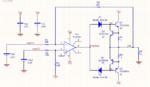
Hi I am trying to design a circuit that accepts as an input 0->5V DC from an AD converter and translates them linearly to -6V to +6V with a maximum sink/source current of 200mA, the input signal will change very slow (every 20ms or more) and the fast response time is not an issue. A have designed and simulated the attached test circuit and I am looking forward for your comments and suggestions, before I prototype the circuit in breadboard. In the simulation the circuit response is excellent but specifically I am worry about the thermal runaway of the two output transistors.
Thanks Nick
8-O
 

Attachments

  • Untitled.png
    Untitled.png
    70.7 KB · Views: 156

I .. worry about the thermal runaway of the two output transistors.

The worst case is @ 5V*125mA=625mW. No problem with a cool-star on each output transistor.
 

You can avoid thermal runaway by biasing output stage as
in B-class audio amplifier.
Look this picture

View attachment B Amp stage.pdf


You can put there even 3 bias diodes and put them in thermal connection
with Q1 and Q2 if needed.
Rb about 2.7k...10k only for bias current for Db.
Now Ube1 and Ube2 are locked together with bias current.
With 3 diodes Ube1-Ube2 is about 2.1V , that is more than safe , but
makes additional crossover distortion.
Look more info about class B amplifiers. (Google)

Regards KAK
 

The only thing you might have to add are some base emitter resistors for Q1 and Q2. 10K will do. This to prevent the transistor from turning due to collector base leakage currents. The base of Q2 is floating when Q1 is on and the base of Q1 is floating when Q2 is on. Biasing into class B or something alike might only be required if you have problems with cross-over distortion. Biasing into class B might need some thermal management to prevent it from running away.

Inventor(y)
 
  • Like
Reactions: NICK7

    NICK7

    Points: 2
    Helpful Answer Positive Rating
You can avoid thermal runaway by biasing output stage as
in B-class audio amplifier.
Look this picture

View attachment 55006

Dear KAK I think that with your suggestion the BJTs will never conduct. But thanks anyway

Inventor I will test your proposal its seams to me reasonable
 

I know this circuit works.
Have made many similar kind of LOFI power amplifiers and powerout drivers
with dual power supply.
You only need to find right values for Rb resistors,
they are non critical. ( related to hfe of output BJT pair.

Check these ............

**broken link removed**

**broken link removed**

Regards KAK
 
Last edited:

Dear KAK your circuit is tested and working!! My mistake!!
Thanks Nick
 

Status
Not open for further replies.

Similar threads

Part and Inventory Search

Welcome to EDABoard.com

Sponsor

Back
Top