Hesambook
Full Member level 2
DC to DC buck converters is a famous topology in the electronic and a widely used circuit in electronic devices. A buck converter steps down the input voltage while it increases the output current. In this article/video, I have discussed a DC to DC buck converter that can be used effectively as a switching power supply. The output voltage and current are adjustable: 1.25V to 30V and 10mA to 6A (continuous). The power supply supports the constant voltage (CV) and constant current (CC) features. Two LEDs demonstrate the CV and CC status. The circuit is compact and both sides of the PCB have been used to mount the components.
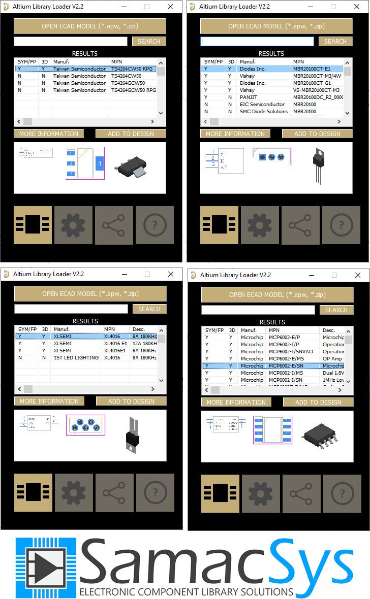
To design the schematic and PCB, I used Altium Designer 21, also the SamacSys component libraries (Altium plugin) to install the missing schematic symbols/PCB footprints. To get high-quality fabricated PCB boards, I sent the Gerbers to PCBWay.
To test the circuit, I used the power analysis feature of the Siglent SDS2102X Plus oscilloscope (or SDS1104X-E), Siglent SDL1020X-E DC Load, and Siglent SDM3045X multimeter. Isn’t cool, so let’s get started!


References
Source: https://bit.ly/2VAxkV5
Altium Designer: https://www.altium.com/yt/myvanitar
SamacSys Altium plugin: https://www.samacsys.com/altium-designer-library-instructions
XL4016 schematic symbol, PCB footprint, 3D model: https://componentsearchengine.com/part-view/XL4016/XLSEMI
MCP6002 schematic symbol, PCB footprint, 3D model: https://componentsearchengine.com/search?term=mcp6002
TS4264 schematic symbol, PCB footprint, 3D model: https://componentsearchengine.com/part-view/TS4264CW50 RPG/Taiwan Semiconductor
MBR20100 schematic symbols, PCb footprint, 3D model: https://componentsearchengine.com/part-view/MBR20100CT-G1/Diodes Inc.
Siglent SDS2102X Plus oscilloscope: https://siglentna.com/digital-oscilloscopes/sds2000xp/
Siglent SDS1104X-E oscilloscope: https://siglentna.com/digital-oscilloscopes/sds1000x-e-series-super-phosphor-oscilloscopes/
Siglent SDL2010X-E DC Load: https://siglentna.com/dc-electronic-load/sdl1000x/
To design the schematic and PCB, I used Altium Designer 21, also the SamacSys component libraries (Altium plugin) to install the missing schematic symbols/PCB footprints. To get high-quality fabricated PCB boards, I sent the Gerbers to PCBWay.
To test the circuit, I used the power analysis feature of the Siglent SDS2102X Plus oscilloscope (or SDS1104X-E), Siglent SDL1020X-E DC Load, and Siglent SDM3045X multimeter. Isn’t cool, so let’s get started!
References
Source: https://bit.ly/2VAxkV5
Altium Designer: https://www.altium.com/yt/myvanitar
SamacSys Altium plugin: https://www.samacsys.com/altium-designer-library-instructions
XL4016 schematic symbol, PCB footprint, 3D model: https://componentsearchengine.com/part-view/XL4016/XLSEMI
MCP6002 schematic symbol, PCB footprint, 3D model: https://componentsearchengine.com/search?term=mcp6002
TS4264 schematic symbol, PCB footprint, 3D model: https://componentsearchengine.com/part-view/TS4264CW50 RPG/Taiwan Semiconductor
MBR20100 schematic symbols, PCb footprint, 3D model: https://componentsearchengine.com/part-view/MBR20100CT-G1/Diodes Inc.
Siglent SDS2102X Plus oscilloscope: https://siglentna.com/digital-oscilloscopes/sds2000xp/
Siglent SDS1104X-E oscilloscope: https://siglentna.com/digital-oscilloscopes/sds1000x-e-series-super-phosphor-oscilloscopes/
Siglent SDL2010X-E DC Load: https://siglentna.com/dc-electronic-load/sdl1000x/